


")

The development of improvised electronic watches are many hams. Most often, for the manufacture of clock used chip CIE (CIE) and CIE. But in hours on these chips is almost always no sound alarm end of each hour. To enter it, having made simple the device, which is described in this article.
Schematic diagram of the device, providing an hourly alarm current time shown in the figure. It consists of D-flip-flop DD1.1. Schmitt trigger on the elements DD2.1, DD2.2 and node management system BQ 1 on the element DD2.3. The detector works as follows. At each change of indications in the ones hours logic level in the low-order binary code on the pin 13 of the chip CIE changes its state to the opposite. A change of state on this pin controls the D-flip-flop DD1.1. To this end the D input (pin 5) plug to the pin 13 of the chip CIE. For recording in the trigger logic levels present at the output, With the input (pin 3) element DD1.1 serves pulses from pin 1 of the chip CIE. Manager discharge units of hours.
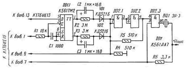
Elements R1C1 provide a slight delay of the pulses at the input S. At the moment each shift readings in the ones place of hours positive differential voltage, arising on any of the outputs of D-flip-flop. by using the chain consisting of capacitor C2. C3 and diodes VD1. VD2. forms on the left (the scheme), the output resistor R4 of the voltage pulse, the duration of which is determined by the values of elements C2, C3 and R4. This pulse is fed to pin 9 of the chip and CIE triggers the alarm generator, the signal from pin 7 of the chip CIE gets on pin 9 of the element DD2.3. And as to the second input of this element (conclusion 8) at the same time will receive a positive pulse from the Schmitt trigger DD2.2, the piezo oscillator BQ 1 will beep, the duration of which is equal the duration of a control pulse, i.e. approximately 0.5 s. Then the output of the Schmitt trigger DD2.2 (pin 4) will be a logic low and the sound emitter BQ 1 stop despite the burst pulse from the generator alarm circuits CIE. entering the pin 9 of the element DD2.3 in for 1 min.
Author: I. Patchin, Fokino Bryansk region.
Addition. In the article "Hourly alarm in hours" (see "Radio", 2000. No. 3, p. 31) we described a simple hourly alarm device designed to industrial or homemade electronic clock on the chip series C. When this, however, was excluded work hours in alarm mode. To save this mode, enough chip CLA be replaced by chip CTS.
Schematic diagram of the modified device shown in Fig. 1. On the trigger DD1.1 assembled as described previously, the device forming the control pulses of the node hourly alarm. Its functions are performed by the key on the element DD2.1. Included same parallel to the key on the element D02.2 controls the alarm that can be turned on or off by the switch SA1.
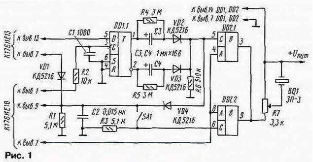
When disabled the alarm (open contacts SA1), the control pulse, generated by the trigger DD1.1, at the end of each hour through the diode VD4 comes on pin 9 of the chip CIE and runs its generator. At this point turn on the key DD2.1 and the signal generator circuits for 0.5 C arrives at the piezo oscillator BQ 1. When the alarm clock (closed contacts SA1) the hourly alarm device will continue to operate, but in his work parallel will participate both keys-D02.1 and DD2.2.
When a clock with the current time coincides with the set-up time the alarm on pin 7 of the chip CIE appears launching the clock pulses which through decoupling diode VD1 is received on pin 9 chip KIE and will include its generator. Formed from launching pulse signal of high level through the SA1 will include key DD2.2 and with its release will arrive on the piezo oscillator BQ 1 you will hear an intermittent alarm. It will sound for 1 min. the Desired volume signal set variable resistor R7.
In the described device it is possible not to install the switch SA1, if multiple to make it complicated. In the clock to display the clock set the alarm on conclusion 11 chips K. IE serves pulses from pin 1 of the chip CIE (Fig. 2). Press the clock button SB1 these impulses through decoupling diode VD5 goes for the pin. 1 trigger DDI .2 and change it state. When a high logical level at pin 13 of flip-flop DDI.2 key DD2.3, replaced the switch SA1 (see Fig. 1). work and resolve the alarm. If button SB 1 transfer trigger DD1.2 low logic level at pin 13, switch will close and the alarm will stop. The differential voltage levels on this (or inverse) output trigger can use to indicate the alarm by using a separate led or ignition decimal points on the display hours (more convenient).
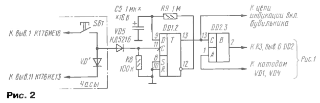
Thus, in this case to control the operation of the alarm is not required to enter additional switch and all its functions will be performed by pressing output button on the indicator of the time display alarm setting.