


")

This simple device allows to increase the reliability your radio equipment and reduce noise in the circuit at the moment of inclusion.
Any supply of radio equipment contains rectifier the diodes and capacitors of large capacity. At the initial moment of inclusion network power pulse occurs, the surge current while the charging of capacitors of the filter. The amplitude of the current pulse depends on the capacitance and voltage at the rectifier output. So, at a voltage of 45 V and capacity 10000 µf charging current of this capacitor can be 12 A. In this case, the transformer and rectifier diodes short work in the short circuit mode.
To eliminate the risk of release of these elements from failure by reducing the inrush current at initial switch-on and serves as shown in Fig. 1.7 scheme. It also facilitates the modes and other elements in the amplifier during transients.
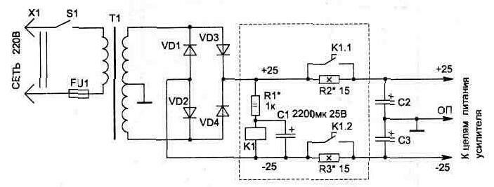
Fig. 1.7
At the initial moment, when energized, capacitors S2 and Sz will be charged via the resistors R2 and R3 limit the current to a safe for details of the rectifier value.
1…2 seconds after charging the capacitor C1 and the voltage across the relay K1 will increase to the point where it would work and their contacts K1.1 and K1.2 will shunt the limiting resistors R2, R3.
In the device, you can use any relay with voltage positives smaller than the effect on the output of the rectifier and the resistor R1 is chosen such that it was dropping the "extra" voltage. The relay contacts should to be calculated on the current in the power circuits of the amplifier peak current. In the relay scheme is applied RES RF4.500.407-00 (RF4.500.407-07 or etc.) with a nominal operating voltage of 27 V (coil resistance 650 Ohms; current, switching contacts, can be up to 3 A). Actually the relay is activated already at 16…17 In, and the resistor R1 is selected a value of 1 kω, the voltage across the relay will be 19…20 V.
The C1 capacitor type K50-29-25V or K50-35-25V. Resistors R1 type MLT-2, R2 and R3 is C5-35V-10 (sew-10) or equivalent. The magnitude of the values resistors R2, R3 depends on the load current, and the resistance can be significantly reduced.
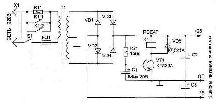
Fig. 1.8
The second scheme, shown in Fig. 1.8 performs the same task, but allows to reduce the size of the device due to the use of timing capacitor C1 less capacity. Transistor VT1 includes relay K1 with a delay after the charge of the capacitor C1 (type K53-1A). Scheme allows instead of the secondary switching circuits to provide a stepped feed voltage to the primary winding. In this case, you can use the relay only with one group of contacts.
The resistance value R1 (sew-25) depends on the power the load is chosen such that the voltage across the secondary winding of the transformer was 70 percent from the nominal value when the resistor (47 300… Ohms).
Setting the scheme is to set the delay time activate the relay the selection of the resistor R2, and the choice of R1.
Schemes can be used in the manufacture new amp or upgrading existing ones, including industrial manufacturing.
Compared to similar purpose devices for two-stage power given in various journals, described here are the simplest.
Publication: www.cxem.net