


")

Readers are provided with a relatively simple dipstick to check health logic circuits, the presence and estimate the duration of the pulse sequences. This, of course, not an oscilloscope, but is simplified a visual representation of logic signals in time very often useful when working with digital devices.
Everyone who works with ICS CMOS or TTL, reliable, and cheap handy device for testing and configuring logical devices. Goal the creation of such a device and was pursued by the author in developing his logical of the stylus. Thus, in pulse matrix oscilloscope [1] envisages measurement amplitude. Actually this property to detect and display unit pulses in common TTL chips and CMOS is not required, I. excluding it. can to significantly simplify the device and reduce its size.
The device, named by the author as a logic probe display (hereinafter referred to probe), allows you to see expanded in time the logical signals and has the following technical characteristics:
- The minimum duration of a detected pulse, ISS......1
- The number of points sampling sweep......24 (48)
- Discrete-time scanner, ISS......1, 10, 20,100, 200
- Supply current when LEDs are switched off (48 points), mA......6,5
- Current consumption at all of the included LEDs and u n and m= 5 In (48 points) mA......160
- Dimensions (excluding needles and switch scanning) mm......180x30x20
- Power adapter - network adapter-stabilized output voltage of 5 V and 9 V.
The device can be used as a source of stable frequency.
The principle of operation of the probe is that the logic levels of the input signal memorized successively in time in the shift register and appear on indicator.
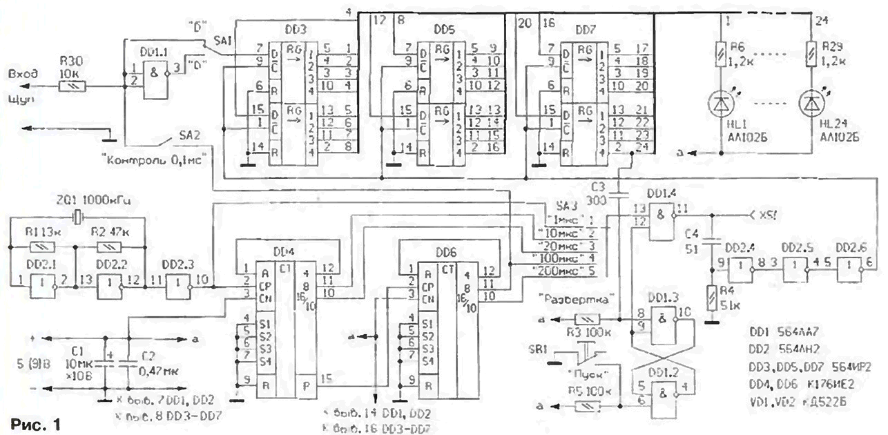
Probe, schematic diagram of which is shown in Fig. 1, consists of a series the following functional units. Sets crystal oscillator at a frequency of 1 MHz performed on the elements DD2.1, DD2.2. frequency divider - on chips DD4 and DD6. A control device consisting of a trigger and start key are collected on the elements DD1.3, DD1.4. The shaper short pulses is made on DD2.4-DD2.6 and C4, R4, the input Shaper is on DD1.1. Serial scan registers are collected at chips DD3, DD5, DD7. The indicator is a line of LEDs НL1 - НL24.
(click to enlarge)
Shown in Fig. 1 diagram of the device corresponds to the embodiment 24 of the countdown, though the author made the probe indicator is on 48 samples and a portion of the information above, refers to the last option. The increase in the number of counts is reached the introduction of additional registers and LEDs.
A crystal oscillator is assembled by well-known scheme. Pulses with a frequency of 1 MHz with o 10 DD2.3 is input to the CP (pin 2) five digit binary-coded decimal counter DD4. It is included in mode decimal divider the use of the fifth grade to increase the range of the sweep. Thus, the counter divides the original frequency of 10 and 20. The inclusion of the counter standard the scheme did not ensure its stable operation. Therefore, the control input CN (conclusion 3) counter connected to the output of the third digit (pin 12), as recommended in [2].Pulses with a period of 1, 10, 20, 100, or 200 mA do through the switch SАЗ ("Scan") to the input of logic element DD1.4. Another its input connected to the RS-trigger, controlled by the button SВ1 "start". When pressed the button allowed the passage of clock pulses through DD1.4. Then these the pulses are shortened differentiating chain С4R4, formed by the inverters DD2.4-DD2.6 and fed to the inputs of the synchronization of registers DD3, DD5, DD7.
Studied logic signals fed to the inverter DD1.1 and, depending on the position of the switch SА1. pass the input information register in the forward or inverted form. With the appearance of the sync pulse to the registers in the first cell (bit) of the register is written to logic level acting in this the moment at its input. During the subsequent recording of reference information about previous is transferred to the subsequent cell. Each chip shift the register consists of two four-digit sections. Therefore, the information input D (pin 15) the following section is connected to the output (pin 10) fourth digit in the last section. Thus, three chip enable registers save 24 reference level logic signal.
Because the CMOS chip have a higher output current in the state log. 0,
the LEDs are connected between the output circuits and the positive power supply. As accustomed to seeing in a glowing indicator high level, in direct mode indication (switch SA1 is in position "D") input signal is inverted element DD1.1.
When the button is pressed SВ1 ("start") information is recorded in the registers after releasing her record ends just after the first of the recorded pulses reaches the last position of the register DD7 and blocks the passage clock pulses by switching through the capacitor C3 trigger trigger DD1.3,DD1.2 in original state.
Assessing the indicator, you need to consider that the status LEDs correspond to the logic levels at the input of the probe to the moments of arrival of the next clock pulses. If the switch SA3 is set in position "1 μs" and glow in a row of five LEDs, the pulse duration of about 5 μs. If the light all the LEDs, it is necessary to move to larger sweep period.
To control the efficiency of the device introduced an additional switch SА2 ("Control 0.1 MS). In this case, the input of the probe serves the pulses from the output 11 counter DD6. They have a duty cycle of 5, i.e. within 20 MS operates the log. 1 and further 80ms - log. 0.
Nest ХS1 in the described embodiment, the probe 24 to the reference used for the issuance of control pulses to check the circuits if I press the "start"button.
The increase in the number of LEDs allows to improve the measurement accuracy the duration of the pulse. The device 48 samples requires three additions chips OR connected similarly to the registers DD3, DD5, DD7 without input inverter. Variant of the probe with the indicator on 48 diodes arranged in two same line, can be used as a dual beam 24 count and how single-beam 48 counts. When connecting the primary and secondary (without inverter) inputs on the one signal and when you turn on one line view of the direct signal and the second inverted signal, the indicator shows the pulse on the oscilloscope screen. When connecting the input an additional block of registers to the output of the 24-th digit of the register obtained the indicator on 48 samples, and the pulse polarity is observed in defined switch SА1.
For TTL chips need a stable 5V supply V.
The details of the design. The probe used LEDs ALBM (in metal the casing) and resistors MLT 0,125. capacitors C2 - km-6, C3 - km-5B, C1 - C50-35 or other small. Quartz - WG-06 at a frequency of 1000 kHz. Button SА1, SА2 and SВ1 - MP7. Switch SАЗ - MPN-1 ten of the provisions or similar. Nest ХS1 - small for pins with a diameter of 1 mm. Possible replacing parts with the appropriate characteristics that likely affect the size the PCB and the housing.
Small chip series have 564 planar conclusions. When replacing the chip it is advisable to choose a series of 164. Part of C no counters IE2, replace analogue from C. Although many chips in this series and work At 5 V, the necessary preliminary verification when decreased food.
The frequency of the master oscillator should not exceed 5 MHz, this limitation is due with a maximum switching frequency for integrated circuits in CMOS. However be mindful of possible inconvenience of counting the pulse duration if not multiple the frequency of the resonator, and more focused on the practice of measurement. For example, if you often have to measure long duration pulses, frequency generator, you can choose specified below, and Vice versa.
PCB to probe with 24 LEDs is presented in Fig. 2. Fee made of two-sided foil fiberglass with a thickness of 1 mm. Transition drill holes are drilled with a diameter of 0.6 mm In Board has two holes with a diameter of 3 mm. Single fastener, the second output jacks; it attached to the top cover. Four holes with a diameter of 1 mm are used for fastening buttons MP7 rivets of copper wire.
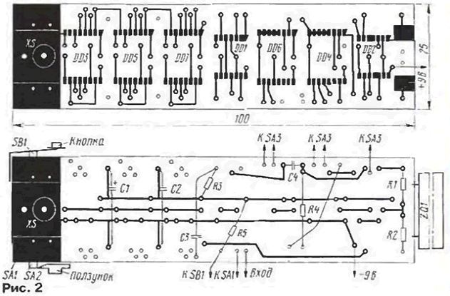
Switch SА1 installed from the back side of the PCB opposite the switch SА2. Two sliders to fix the micro-machined needle files from plastic. The spring for the button SВ1 made of the contact plate relay type RPU start button - from the PCB.
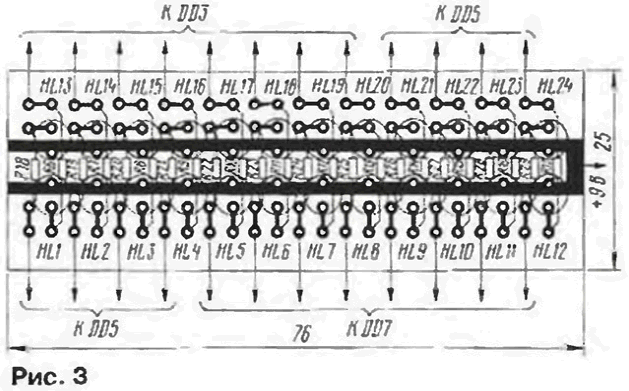
In Fig. 3 shows the printed circuit Board of the led (24 LEDs) the arrangement of elements on it. During installation, first install the LEDs so. their housings are not in contact, then by printed conductors sealed resistors.
Housing glued with epoxy from fiberglass. In the case done the holes for mounting the probe, sliders, switch, and three holes for the mounting screws. They are installed as follows: one in the center, and it fixed Board with components, the other two at the edges. In the attachment Board a contact area through which the screw is connected to a common power bus. Under the nut of the screw is attached a wire with an alligator clip to connect to a shared wire investigational device.
The mounting device is made of wire MGTF-0,07. Fee set in case elements down, stacked on top without fixing charge indication and press it a top cover having holes for the LEDs. With power supply probe is connected wire Mgtf-0,07.
Literature
Author: N. Zaets, Belgorod region