


")

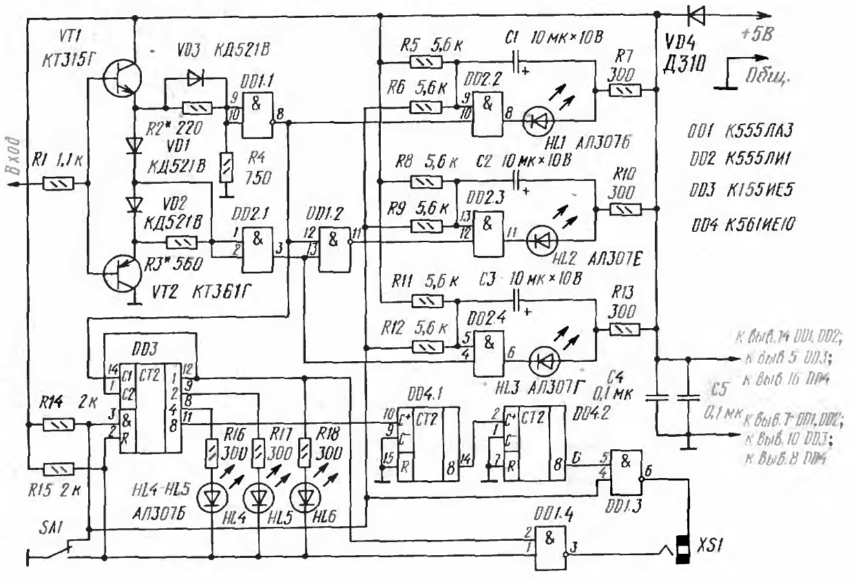
Those who have to establish electronic devices collected on digital the TTL chips that may use a logic probe, principled the diagram of which is shown in the figure. In some cases it can even replace oscilloscope. The device is characterized by small dimensions, low power consumption and easy handling. It is convenient to use when searching for defects in the blocks, located in remote places, especially in the repair outside the Studio.
Unlike many other designs of the probe allows you to define and display three colored LEDs are not only the voltage levels 0 and 1, but an intermediate level. Time display short pulses of all three levels increases to 0.1, which ensures their visual observation. If desired increasing the pulse duration can be turned off and then on the brightness of LEDs can estimate their duty cycle and Squareness. To determine the number came pulses probe equipped with a counter for 8 with three indication single-color LEDs.
The probe also allows "listening" to judge the frequency of the test signal. For this is fitted with a socket for connecting the phone to the output of the divider by-2 frequency (audio frequency) or to the output of the frequency divider to 4096 (for high frequencies up to 10 MHz).
(click to enlarge)
Specifications
- The indicated voltage levels In: zero (0)......0…0,4
- intermediate ......0,4…2,4
- one (1) ......2.4 GHz 5…
- Input resistance, Ohm, not less......40
- The duration of the studied pulses, MS, no less......50
- Current consumption, mA, not more ......70
Input device tester is an emitter follower on transistors VT1 and VT2. Resistor R1 protects it from overloads when submitting signal with a voltage higher than the supply voltage, or pulse negative polarity. Diodes VD1 - VD3 and resistors R2-R4 determine the thresholds actuation of the elements DD1.1 and DD2.I. The selection of the resistor R2 is set lower the limit designated level 1, and the selection of the resistor R3 is the upper limit level 0. The elements DD1.1 and DD2.1 form a steep front and a decline pulses. The element DD1.2 defines an intermediate level of the test signal.
LEDs HLI - HL3 show respectively the level 1, intermediate voltage and level 0. These LEDs are connected to the outputs of single vibrators on the elements DD2.2 - DD2.4. In the shown position of the switch SA1 single vibrators lengthen short input pulses arriving at them, so the duration at which the illumination of the LEDs noticeably eye. When switching switch SA1 in the bottom on the diagram the position of the resistors R6, R9, R12 are disabled from the common wire and through a resistor RI4 entered level 1 that translates single vibrators in mode repeaters. With increasing duration pulses does not occur. In this position of the switch the led glow HL2 the brighter, the more the duration of the rise and fall of the studied pulses. If they almost rectangular, led HL2 is not lit.
Since the input C1 of the counter DD3 is connected to the exit of the element DD1.1, the counter counts the number of pulses 1. He can count them on level 0, if you switch this input the counter to the output of the element DD2.1. The outputs of the counter is connected LEDs HL4 - HL6, each of which displays the status of its corresponding binary discharge. The number of received pulses is equal to the sum of weights of outputs counter corresponding to each of LEDs HL4 - HL6 (respectively 1, 2 and 4 of the pulse). Every eight pulses of the count cycle repeats. Counter reset occurs during the switching time (span) contact switch SA1, as only in this time interval both the inputs R counter there is level 1. With the aim of reducing current consumption in the diagram shows the position of the switch SA1 LEDs HL4 - HL6 not glow.
To the output 8 of the counter DD3 serially connected counters DD4.1 and DD4.2. The total division ratio of the frequency of the three counters is equal to 4096. Pulses output 1 counter DD3 served on one of the inputs (pin 2) of the element DD1.4, and the pulses output from the 8 meter DD4.2 - on one of the inputs (pin 5) of the element DD1.3. In the shown position of the switch SAI element DD1.3 is turned off and the element DD1.4 is enabled (at pin 1 is present level 1). Consequently, the phone pass pulses with a frequency that is two times smaller than the input probe. This is necessary to ensure that the duty cycle in the phone was equal to two regardless of the duty cycle of the studied pulses. When you switch the switch SA1 in the bottom on the diagram the position of the element DD1.4 is closed, and on the phone receives pulses from the output of the opened element DD1.3 with a frequency of 4096 times smaller than the input probe, which allows to monitor the input pulses frequency up to 10 MHz.
Diode VD4 protects the tester from incorrect connection to the power source. Capacitors C4 and C5 block the impulse noise on the food chain, they should be allocation to different points in the chain (evenly).
The body of the probe serves as a pencil case from collet pencil sizes HH mm. All parts are mounted on the Board size HH,5 mm installation completed wire MGTF was 0.12.
In the probe chip series K555 can be replaced by a similar series K155, but thus, the current consumption will increase by half. Diodes CDV (VD1 - VD3) you can replace CD, CD, CD, KD521, KD522 with any letter index. The LEDs will fit any other, both by type and by color. Instead transistor CTG you can apply CT, CT, KT3102, etc., and instead CTG- CT, KT3107 and others, also with any letter index. The diode can D replace DA. Resistors - MLT, capacitors C1 - C3 - C50-6, C4, C5 Km-5. The switch SA1 can be any small, however, convenient to use switch PGM-1, because its design allows the counter in repaired slight pressure on the handle without taking it to another extreme fixed position (when the force is removed, the handle returns to its original position).
The input probe is made of cut (threaded) from a Bicycle spoke length 50 mm, is fixed at the front end of the body two nuts M2. On the opposite end of the body there is a slot for your phone TM-2, and in the hole removed the wires for applying voltage to the study device.
Author: Y. Yuditskii, Gomel