


")

Level switch environments (hereafter WMS) is designed to indicate the presence of certain objects (solids, objects) in the immediate vicinity of the sensor (sensing element). In fact, it is capacitive relay, annunciator changes in the capacitance of the capacitive sensor. From such devices resonant type, the WMS is characterized by the absence of inductors and ease of use. This schematic provides a response to the capacitance change of the sensor only 0.5 pF (!). This allows you to react to the approach of a person's palm at a distance of 5-8 cm to the sensor surface.
Flowchart WMS is shown in figure 1, and consists of: sensor - 1, clock - 2, reference generators -3 and -4 measuring signals, comparing the device - 5, a matching - 6 Executive and 7 devices and power supply - 8.
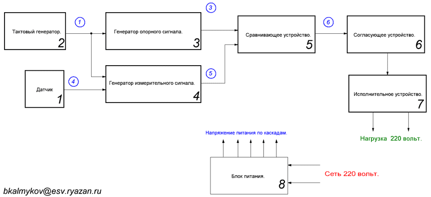
Fig. 1
Consider the circuit in figure 2:
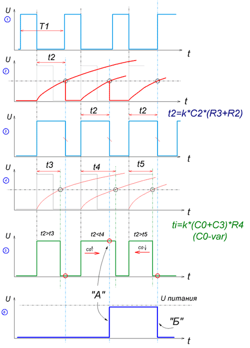
Fig. 2
The clock generator produces clock pulses (1), which runs a support (3) and measurement (5) waiting multivibrators. The duration of the reference pulse detect circuit elements (3), (can be changed manually). The duration of the measurement pulse (5) depends on the capacitance of the sensor.
In the initial state, when the sensor is not exposed to foreign objects, its capacity is small and the duration (t2) of the reference pulse that is longer than the length measurement (t3) of the pulse (t2> t3, figure 4, 5). At the approach of the controlled object to the sensor electrical capacity increases, the duration of the measurement pulse (t4) increases and at some point becomes more basic (t2) (t2<t4, Fig. 5). Comparing the device detects the change of the inequality sign and signal synchronization remembers this state (point "A" in diagram 5 and 6). Depending on this, matching and actuators, connect the load to the mains 220 volts.
While the distance of the controlled object to the sensor, the capacitance decreases and the duration of the measurement pulse is reduced (t5) and when it will be less than t2 , the circuit will return to its original state and with load the voltage will be removed (point "B" in figure 6).
Consider the schematic diagram of the detector WM figure 3:
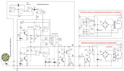
Fig. 3 (click to enlarge)
The oscillator is assembled on the logic elements DD1. The reference signal generator implemented on 2 elements DD2, VT1 transistor and timing chain C3, R2, R4. Its parameters are adjusted by the resistor R4.
Measuring the generator signal is performed on the remaining 2 elements DD2, the transistor VТ2 and timing chain C0,C2, R3. The outputs of both oscillators is applied to terminals "D" and "C" trigger DD3. When the pulse width of the measuring channel (5) is greater than the pulse width of the reference channel (3), a trigger is written to "1" (6). To agree on the level of the signal is performed in the matching device 6 (Fig. 1), collected on elements:VТ3, VТ4, R13, R14, R16-R18 (Fig. 3). Relay cascade actuating device 7 is assembled on VT5. The relay contacts K1 commute power to the loads. In the upper part of the diagram represents semesterly variant of the switch load. Both schemes do not have features.
The design of the WMS and the sensor shown in figure 4.
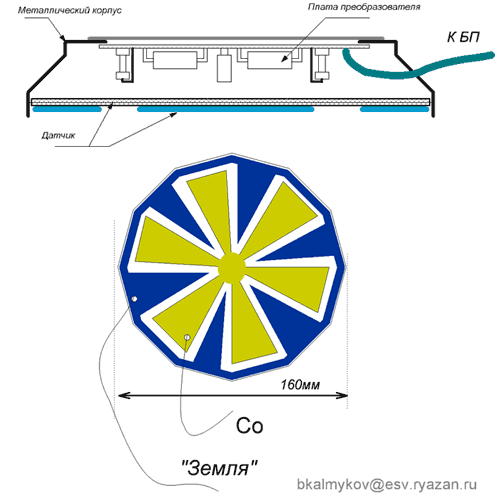
Fig. 4
The supporting member is a metal case accommodating a disk of foil PCB thickness of 1.5 mm and a diameter of 160mm. The pattern of the sensor caused by the paint on the stencil. Unprotected areas etched, the resulting zones (the capacitor plates of the sensor) solder wires to connect to the schema.
The setting of the indicator is to test the voltage of the power circuits and the control of conformity of the signals at the test points in accordance with figures 2 and 3. When the initial state of the sensor pulse width at pin 3 of chip DD3, must be less than the pulse duration of the output 5 of the same MS. This is achieved by adjustment of trimmer resistor R4. Hands on approach to sensor output 1 chip DD3 needs to be a transition from "0" to "1". The sensitivity is specified with a slight change of the position of the resistor R4. Configure the rest of the circuit, and with proper details, not required.
Structurally, the detector is constructed from two blocks (highlighted in figure 3). Left (the scheme), some specimens were collected in the vicinity of the sensor in one housing. The right part - a separate unit. The connection between blocks 3-wire, no limited length (within reason).
The questions investigators will answer bkalmykov[собака]esv.ryazan.ru
Author: Kalmykov, B. M.; Publication: www.cxem.net