


")

The structure of the field detector includes a high-pass filter, RF amplifier, diode detector, a DC amplifier with a logarithmic dependence of the gain, sound generator with variable frequency and scale led 12 LEDs. A detector capable of detecting radio microphones operating in the frequency range 20-600 MHz. Schematic diagram of the device shown in the figure.
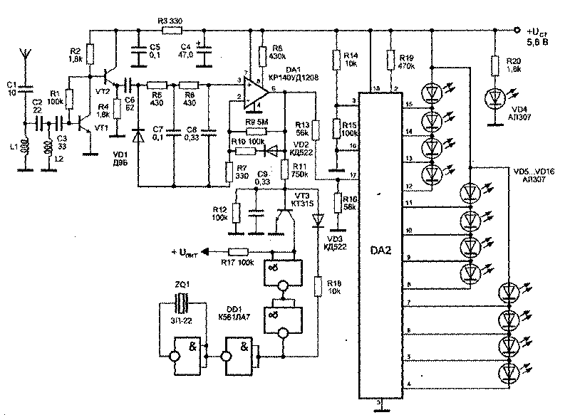
The signal induced in the antenna is filtered HPF on the elements of C2,L1, NW, L2 and fed to a broadband aperiodic amplifier. Last performed at a high frequency transistor VT1 type CT. The load of the amplifier is the emitter-follower transistor VT2 type CT. The signal taken from the sensitivity of the resistor R4 flows through the capacitor C6 to the diode detector, assembled the diode VD1 type DB. High-frequency components are filtered by RC filters R5, R7 and R6, C8. Low-frequency signal fed to the amplifier on the chip DA1 type CRUD. The gain of this amplifier is determined by the value of resistor R9. When a low level input signal amplifier DA1 has a large gain. Increasing the signal the opening of the diode VD2 type KD522, the resistance of which varies in a logarithmic law. This leads to a change of the resistance of the feedback is also logarithmic. From the output of the amplifier on the chip DA1 signal is supplied to the led indicator and a sound generator.
A sound generator is made on the VT3 transistor KT315 type and DD1 chip type CLA. Capacitor C9 is charged through resistor R11 to the voltage of opening of the transistor VT3. This leads to a change of logic level one to logic level zero at the collector of the transistor VT3. The cathode of the diode VD3 type KD522 is connected through a resistor R18 to the negative pole of the power source. Capacitor C9 is quickly discharged through the circuit VD3, R18,which results in the closing of the transistor VT3. Capacitor C9 again begins to charge and the whole process repeats. Rectangular pulses are converted piezoceramic transducer ZQ1 type SN-22 in sound. If you increase the voltage on the output of the amplifier DA1 decreases the charging time of the capacitor C9 to the stress of opening of the transistor VT3, and this, in turn, leads to an increase of the pulse repetition frequency of the generator. Thus, by increasing the level of the input signal is an increase in tone.
The basis of the led chip is DA2 type CMP. The chip is CMP specialized and performs the function of control scale, providing shaded columns on the scale of 12 LEDs that light up sequentially when the input voltage from the minimum to the maximum value. The brightness of the LEDs is kept constant. Input, via the voltage divider resistors R13, R16, is fed to the input circuit DA2 (pin 17). On pins 16 and 3 chip DA2 serves the reference voltage levels that define, respectively, the minimum (the LEDs are not illuminated) and the maximum (all the LEDs are lit) the values of the input signal. The device is powered by the power source voltage of 5.6 V. the Led VD4 type AL307 is to display the switch device.
All used items small. Details HPF as described above. DA1 chip can be replaced by CRUD or any other operational amplifier with its correction circuits. Instead of DD1 chip can be applied CLE. When replacing the diode VD1 on GD range of the device can be increased up to 900 MHz.
Publication: www.cxem.net