


")

We offer our readers a dimmer allows you to adjust the brightness lighting in rooms, power appliances, heating elements, speed of rotation of AC motors. It can be used to reduce inrush current of lamps, nakalivanija, which prolongs their service life. Dimmer control buttons that gives you the ability to enable and disable the load appreciable distance from the controlled object. And that button was to find in the dark, next to her is established, the led illuminates only when you turn off the light.
This regulator is made on the basis of the device described in the article S. Biryukova "Triac power controllers" ("Radio", 1996, No. 1, pp. 44 - 46). Unlike he proposed in this article, the dimmer is not turned off completely network, requiring its completion for the purpose of reducing current consumption. In the resulting current is decreased to 1.5 mA in all modes of operation. After processing expanded the range of power control. When stavatti load it is about 99%.
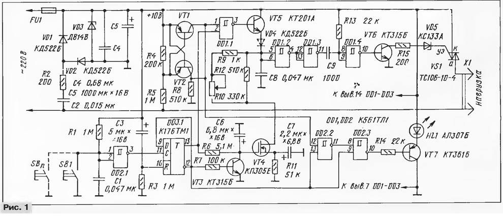
Schematic diagram of the dimmer shown in Fig. 1. To manage the triac VS1 necessary shaper short pulses, one of the conclusions of which is connected to a network wire. Powered driver from source collected on elements C2, R2, VD1 - VD3, C4, C5. Diodes VD1, VD2 perform the function of the rectifier. Rectified voltage is stabilized at the level of 10 In Zener diode VD3. Capacitors C4, C5 are part of the smoothing filter, and C4 basically bypasses high-frequency interference, which is not suppressed oxide capacitor C5 due to its significant parasitic the inductance.
(click to enlarge)
If a positive voltage on the anode of most triacs can be opened pulses any (relative to the cathode) polarity, managing incoming electrode and the negative pulses of negative polarity. The positive terminal of the power source of the described controller is connected to the cathode of the triac. At the control electrode will be formed negative pulses of any polarity at the anode.
When using pulse-phase method, the power in the load is controlled by the changes are part of the half cycle of the mains voltage, during which the triac skips the current. It is necessary to distinguish the beginning of each half cycle line voltage corresponds with the voltage equal to or close to zero), and then within 10 MS (the duration of a half period of the mains voltage 50 Hz) itself to form a control pulse. Thus, the earlier will open the triac, the more power will be allocated to load.
The pulse shaper 100 Hz assembles the elements of VT1, VT2, R4, R5, R8. During the positive half cycle of the mains voltage transistor is open VT1, during the negative - transistor VT2. Resistor R5 limits the base current of the transistors. Resistor R8 performs the functions of both the collector load transistors. When the mains voltage is close to zero, both transistors are closed and the voltage at their collectors is equal to the voltage at the negative output of the source power. While the input 1 of the element DD1.1 the formation of short pulses negative polarity corresponding to the beginning of each half cycle network voltage.
When enabled the controller to the input 2 of the element DD1.1 present voltage corresponding to a high logic level, so a negative the pulses at the input 1 of this element are inverted them and arrive at the base transistor VT5, enabled by an emitter follower. Flowing through the current charges the capacitor C8, almost to the voltage of the power supply. Discharges the capacitor through the circuit R9, R10, R12, VT4. When you discharge it to voltage threshold, the switch elements DD1.2 and DD1.3. The voltage drop that occurs at the output 11 of the element DD1.3, is differentiated by the circuit C9R13 and in the form of a pulse duration of about 12 μs from the inverter DD1.4 is supplied to the current amplifier transistor VT6, and then to the control electrode triac VS1. Variable resistor R10 regulate the duration of discharge capacitor C8, which determines the moment of switching on of the triac, and hence the effective voltage at the load.
Zener VD5 provides reliable starting dimmable devices. When his absence in the first moment you turn on the controller after the break through managing the transition of the triac and transistor VT6 current begins to flow, not giving to charge the filter capacitor C5 and preventing the growth of tension the power supply to the nominal value. Resistor R15 limits the current through managing the transition of the triac. The need for such a limitation is not due the safety operation of the Zener diode and triac (short the current pulse can not put them out of action), and possible deterioration of the economy dimmer.
On the inverter DD2.1 and the trigger DD3.1 assembled device power on and off of a dimmer switch, transistor VT4 - smooth switching node load, and on the elements DD2.2, DD2.3, VT7, HL1 - a site highlighting the buttons SB1 (SB2 - SBn).
When you initially turn on the controller, or after loss of mains voltage chain C3R3 generates a positive pulse at the input R of the trigger DD3.1, setting it to the zero state in which the load is turned off. Item DD3.1 responds to a positive differential voltage at the input and With each time the appearance changes its state to the opposite. Chain R1C1 suppresses contact bounce button SB1. Through the resistor R1 also sets the voltage on the input of the inverter DD2.1. When you press the SB1 output of this element occurs a positive voltage drop, switching trigger DD3.1 in one state. High logic level appearing at the same time on direct the output of the trigger, enables the logic element DD1.1. At the same time through the resistor R6, the capacitor C6 is charged almost to 10 V. as you grow the voltage on this capacitor increases the voltage on the gate of the transistor VT4 and smoothly decreases the resistance of its channel, reaching a minimum after 5…7 with after the start of charging of the capacitor C6. And since the channel of the transistor VT4 in series with the resistor R10 in the circuit discharge of the capacitor C8, power in the load gradually increases to the level set by resistor R10.
Resistor R11 creates minimal negative bias on the gate of the transistor VT4, which provides a complete shutdown of the dimmer at zero the resistance of the resistor R10. This offset is necessary to ensure that when turn on the light immediately goes off load. Capacitor C7 bypasses resistor R11 DC voltage, eliminating it from the circuit discharge capacitor C8.
Low voltage with inverse input of the trigger DD3.1 closes the transistor VT3 and prevents switching inverters DD2.2 and DD2.3. As a result, the transistor VT7 is closed, the current is not flowing through it and its emitter included chain HL1 led is not lit.
The next time you press the SB1 (SB2-SBn) trigger switches back to zero state. A logical zero since its release 13 prevents switching element DD1.1, and the output of the latter is set to a logic high the level of that support open state of the transistor VT5. As a result the capacitor C8 is charged to the maximum voltage, and the load is de-energized. Present at this time, the output 12 of the trigger a logic level zero open the VT3 transistor through which will quickly discharge the capacitor C6, and the dimmer is ready for a new integration. High logic level of the voltage output 12 of the trigger, will also be added to the inputs 13 and 9 logical elements DD2.2, DD2.3 and will allow them to skip the negative pulses load transistors VT1, VT2. These pulses will open for a short time the transistor VT7, and included in the emitter circuit of HL1 led is flashing. Resistor R14 limits the average current through the led, so as not to overload power source, otherwise its voltage will begin to fall.
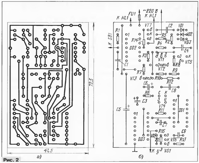
All the details of a dimmer switch, in addition to the triac VS1 and LEDs HL1, mounted on the PCB of one-sided foil fiberglass. Drawing Board shown in Fig. 2, and the location of the parts in Fig. 2, b.
During installation, you can use fixed resistors C2 - OPA, or MLT, and any variable resistor specified on the concept of resistance. Capacitors C1, C2, C8 - K73-15, C - 3 and other series K70 - K, capacitor C2 must be rated for a voltage of less than 250 V. the Capacitor C3 is any oxide, C4, C9 - ceramic km - 5, K10 - 17, C5 - C50 - 24 or K50 - 29, C6, C7 - K53 - 14. In place of the diodes can work CD, CD with any letter index. The Zener diode VD3 - any voltage stabilization 10 V. Transistors VT1, VT2 can be any low-power silicon structure p-n-p with the current transfer ratio of more than 100. Transistors VT3, VT6, VT7 - low-power silicon, VT5 - series CT with any letter index. Also suitable silicon low power transistors of the structure n-p-n, but in this case it is necessary to include in the device, diode VD4, shown in the diagram by a dotted line. Diode protects the emitter junction from reverse breakdown voltage appearing on it each time after closing of the transistor VT5. Field-effect transistor of the series with K any letter index. Fuse FU1 shall be rated for a current of less of the load current.
The adjustment of dimmer is reduced to the selection of the resistor R11. First of all break the chain connecting pin 2 of the element DD1.1 and pin 13 of flip-flop DD3.1. Then conclusion 2 DD1.1 connect with his conclusion 1. After that, the engine of the R10 set in the lower according to the scheme position. In place of the resistor R11 include variable resistor a resistance of 100 ohms, and set the engine in such the position in the circuit resistance is zero. Next, include the dimmer in the network and wait until the power supply output will not install the nominal voltage of 10 V. Then, monitoring with an oscilloscope form pulses of current in the load, increase the resistance of the variable resistor (R11) until then, until the triac VS1 will not open. Since then, several times switch on and off the load securely each time checking whether the transistor VT4 closes the triac VS1. Then a variable resistor constant and replace re-connect output 2 of the element DD1.1 with the output 13 of the trigger DD3.1. If desired, the installation and the selection of the resistor R12 can be achieved to the maximum resistance of the resistor R10, working as a rheostat, consistent with zero voltage at the load.
That at full load on the triac fell as little as possible the voltage, it should be opened as soon as possible after the start of halftime. For this pulse shaper transition of the mains voltage through zero should to produce relatively short pulses. Minimize them achieve selection resistors R4 and R8. To reduce the resistance of the resistor R5 is undesirable, as TCEs it will increase power consumption.
The dimmer has such a nice feature: if the load was on, after momentary power loss in the network (at the time less than 2 min) it turns back on. This is because the capacitor C5 in the filter power drain very slowly, so that none of the logical element will not be switched.
When establishing a dimmer and its practical use remember that all of its elements, including the axis of the variable resistor, are under the mains voltage.
To limit the current through the led HL1 resistor R14 is advisable to move from the base circuit of the transistor VT7 in the circuit of emitter, reducing the resistance R14 to 0.5…1 kOhm.
Author: A. Rudenko, Kharkov, Ukraine