


")

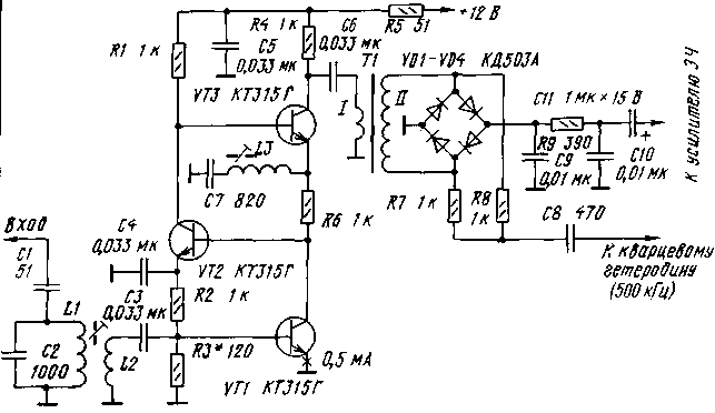
Fig.1
The amplifier is assembled on transistors VT1-VT3, galvanically interconnected. The quiescent current of all three transistors is set automatically and depends on the resistance of the resistor R3. Any changes in the mode of one of the transistors (e.g., temperature fluctuations) immediately lead to changes in the other mode, and quiescent current is restored to its previous value.
As can be seen, the input of the amplifier included parallel resonant circuit L1C2, and in the emitter circuit VT3 - to-serial circuit L3C7. The load is balanced ring mixer diodes VD1-VD4. Approval of last input impedance with the output impedance of the amplifier is performed by the transformer T1. Chain R5C5 protects your device from interference on the food chain.
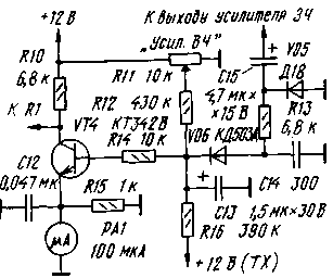
Fig.2
Optionally, the device is easy to introduce a gain control, using, for example, the circuit shown in Fig. 2 (the numbering of parts on it and subsequent figures continues in Fig. 1). In this case, the upper (the scheme), the output resistor R1 is disconnected from the supply circuit and is connected to the collector of transistor VT4. The gain adjust variable resistor R11. Microammeter PA1 is used as an S-meter. When feeding on the bottom (Fig. 2) the output resistor R16 voltage +12V amplifier closes (gain tends to zero). The need for this arises during the transmission, when used in the transceiver.
Coils L1-L3 is wound in bulk on a plastic frame with a diameter of 5 mm with trimmers carbonyl iron from the shell-type magnetic circuits SAT-9a. If equal to 500 kHz, coils L1 and L3 must contain 70 turns of wire PEL of 0.24 and L2 - 20 turns of the same wire, wound on top of L1. As the RF magnetic circuit of the transformer T1 uses a ferrite (NN) an annular magnetic core size CHH. Its winding I (45 turns) and II (15 turns) wound wire PELSHO of 0.24.
Configure the amplifier to the input signal selection resistor R3 to obtain the current of the emitter of the transistor VT1 is equal to 0.5 mA. Then the input signal frequency 501 kHz and by changing the inductance of coils L1 and L3 by moving the trimmers, achieve maximum 3H signal at the output.
The amplifier can be used for other if frequencies. Thus, when the inverter is equal to 5 MHz, the coils L1, L3 and L2 must contain respectively 31, 31 and 5 turns of wire PEL 0,24, windings I and II of the transformer T1 - 15 and 5 turns PELSHO of 0.24. The capacitance of the capacitors C2, C7 in this case must be equal to 100, S4 - 1200 pF, and C3-0,015 UF.
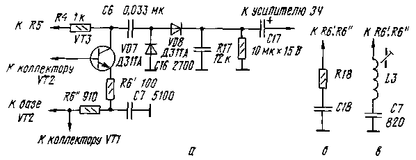
Fig.3
In Fig. 3, and shows the wiring to the amplifier, the amplitude detector. When the FC 500 kHz the values of capacitors C7 and 16 are respectively equal to 5100 and 2700, when the inverter 5 MHz - 1200 and 270 pF.
To obtain the desired frequency response instead of the capacitor C7 is used series circuit R18C18 (Fig. 3,b) and L3C7 (Fig. 3, in). By changing the parameters of its components, it is possible to change the resonance characteristic of the amplifier over a wide range. Bandwidth (and simultaneously gain) govern the selection of the resistor R6 . In this case the total resistance of resistors R6' and R6 must remain equal to 1 kω.
When replacing the circuit L3C7 capacitor 0,033 UF and excluding L1 C2 amplifier becomes broadband with a slight rise of the frequency response in the region of 500 kHz. When replacing C4 and contour L3C7 capacitors capacitance 1200 pF small recovery response observed in the region of 5 MHz.
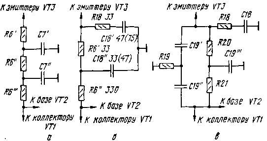
Fig.4
To obtain other characteristics instead of the resistor R6 (and optionally R2) you can use the circuit diagram of which is shown in Fig. 4. For example, the circuit scheme in Fig. A 4.6 will help to form the characteristic double-peaked with a slight dip in the middle. To do this, one such circuit (the values of capacitors C18' C18" listed outside the parentheses) include instead of R2, and the other (with the values specified in brackets) - instead of R6 and simultaneously exclude the elements C4, L3 and C7. The bandwidth of the amplifier with such refinement - 25…40 MHz. The nominals of elements introduced chains, "resonance" characteristics of the amplifier can be shifted in the frequency band from ham.
When using the chain, made by the scheme in Fig. 4, the frequency response of the amplifier is determined by the frequency of quasi-resonance double T-shaped bridge R19C19C19"R20R21C19"'. The quasi-resonance frequency f is calculated by the formula: f = 1/2пRC, where R is the resistance of the resistors R20, R21 (1K); R19=0,5 R =510 Ohms; C - capacitance capacitors C19 , C19", C19"=2C.
Chain R18С18 plays the role of additional selective element, correcting the overall frequency response of the amplifier.
With a suitable choice of the elements of the correction circuits of the amplifier can operate in a wide frequency range from several tens of kHz to 150 MHz (of course, when using the respective transistors). Bandwidth when using LC-circuits - 10 kHz (the minimum value), when using RC-circuits - up to 100 MHz (the maximum value).
Note that the exclusion from the amplifier capacitors C4, C7 observed adverse quasi-resonance in the frequency range 200…500 MHz due to the influence of parasitic capacities.
Author: Vladimir Rubtsov (UN7BV); Publication: N. Bolshakov, rf.atnn.ru