


")

The disadvantage of frequency doublers, often used in digital systems is the need to customize for each specific frequency. The proposed scheme is intended for use in the divisors of N, does not require any adjustment in the range from 0 to several megahertz.
With the passage of the signal through the circuit in each inverter, in addition to the inversion pulse, introduces a small delay (typically 20 NS). For example, the signal at point D is inverted after 60 NS after inverting the input signal at point L, hence both the inputs of gate 6 high potentials remain within 60 NS after the switching of the input signal at point a from low to high. In this case, the output voltage of the valve 6 (point F) is reduced after 60 NS after the arrival of the positive differential input of the circuit. Almost a similar process occurs in the valve 5; the only difference is that its output is low potential is formed within 60 NS after the arrival of the negative differential input. In the circuit shown in the figure, the inverters 1, 2 and 3 serve a dual function in the formation of negative pulses of 60 NS at points F and G. This circuit design can reduce the number of valves.
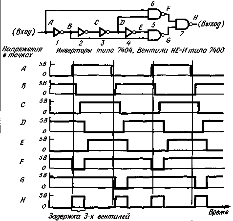
Output pulses of the valves 5 and 6 are fed to the inputs of gate 7', which forms a positive pulse 60 NS with a reduction in the capacity on any of its inputs. Decreasing the voltage on one input coincides with the rising edge of each input pulse at point a, and decreasing the voltage at the other input coincides with the falling edge, so the frequency of the output pulses at point N is doubled relative to the input at point A.
Author: N. Machachi; Publication: N. Bolshakov, rf.atnn.ru