


")

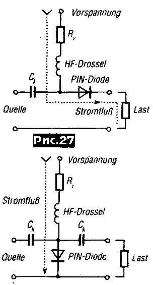
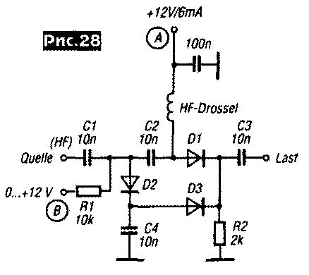
In a sequential scheme, the diode passes the signal from the source to the load in an open state when applying the appropriate bias voltage, while parallel in the open state, the diode bypasses the signal source, closing on a common wire capacitors of the IC. In Fig.28 shows the combined scheme switch on D1, similar to Fig.27, and the attenuation element D2, D3. When applying bias to the point And the attenuation between the signal source and the load is minimal. If in point In file >0…+12 V, the current will flow through R1, D2, D3, R2, and depending on its magnitude will change the resistance of D2, wherein the portion of the RF input signal is shorted to ground through C4.
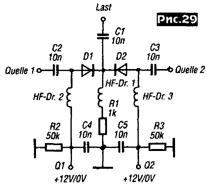
Simple switch the two RF signals shown in Fig.29. When switching this scheme, filters, mixers, etc. should be taken into account that at the moment from two sources can only be activated by one and the other should be grounded.
The resistance R1 is determined by the type of PIN diode. PIN diodes can be used as antenna switches transmission/reception (Fig.30).
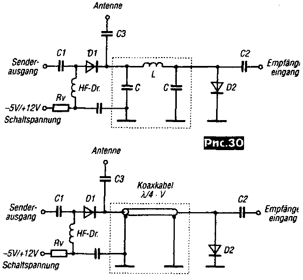
Usually between the receiver input and the transmitter output is switched quarter-wave transmission line or similar length coaxial cable (Fig.30, bottom), and LW - U-shaped LC analog quarter-wave line (Fig.30, top). The values L and C of this chain are calculated by the formulas:
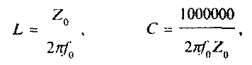
where Zo is in ohms, f is in MHz, L is in µh, C is in pF. At the operating frequency of 28 MHz, the impedance of 50 Ω we have L=0,28 µh and the two capacitors on 113,7 pF. Power loss is calculated by the formula:
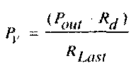
When the output power of 20 W, the resistance of the diode D1 during the live broadcast at 0.5 Ohms power loss would be 0.2 watts. If the CWS (S) at the output significantly greater than 1, the power losses taking into account the CWS (S) can be determined by the formula:
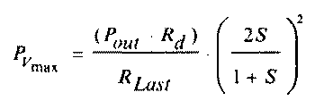
For example when KCB=S=3, we can expect power loss of 0.45 watts. Thus, it becomes possible to apply in QRP transceivers widespread PIN-diodes. The use of switches, PIN-diode significantly reduces the time to switch from reception to transmission, which is especially important when working digital modes connection. In receive mode to eliminate intermodulation distortion D2 is important to lock the PIN diodes, submitting a negative offset for the schemes in Fig.30
Author: Max Perner, DM2AUO; Publication: N. Bolshakov, rf.atnn.ru