


")

In the present article describes the switching Converter to power electronic devices voltage of 5 V from the AC. The Converter does not contain scarce and expensive, easy to manufacture and the establishment.
The power supply has protection from shots of the output voltage and overload current with automatic return to operation mode after its removal.
Main technical parameters
- Input voltage, V.....150 240…
- Input voltage frequency, Hz......50…60
- Conversion frequency, kHz......100
- Output voltage, V......5
- The amplitude of the output ripple voltage, mV, not more......50
- The load current, And......0…6
- Ambient temperature, °C......-10…+50
- The static instability of the output voltage when the input voltage, load current and ambient temperature in full interval % from the nominal value, not exceeding......3
- Dimensions, mm......60x95x30
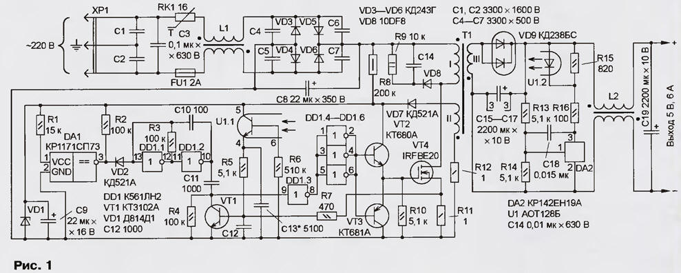
In Fig. 1 shows a diagram of the device.
(click to enlarge)
The management node implements pulse width the principle of stabilizing the output voltage. On the elements DD1.1, DD1.2 holds a master oscillator operating at a frequency of about 100 kHz if the signal ratio is close to two. Pulses with a duration of about 5 microseconds through the capacitor C11 to the input element DD1.3, and then amplified current connected in parallel with elements DD1.4 - DD1.6. To stabilize the output the voltage of the power source, the pulse duration during adjustment reduced. "Shortens" the pulses of the transistor VT1. Opening each period operation of the generator, it enforces the input element DD1.3 low level. This state is held until the end of the next period is exhausted capacitor C11.
Transistors VT2, VT3 made a powerful current amplifier that provides the rapid switching of the switching transistor VT4. Chart voltage on the main elements of the power source during the run shown in Fig. 2.
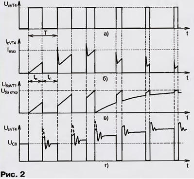
When the transistor VT4 is open, the current flowing through it and the winding I transformer T1 increases linearly (Fig. 2,b). Pulse voltage from the sensor current through the resistor R11 R7 is supplied to the base of the transistor VT1. To exclude false opening of the transistor, the emission current of the smoothing capacitor C12. First after running several periods of the instantaneous voltage on the base of the transistor VT1 there is less tension the opening Uбэ open - 0.7 V (Fig. 2, in). Once instantaneous voltage during another period reaches 0.7 V, transistor VT1 appears that, in turn, will lead to the closing the switching transistor VT4. Thus, the current in the winding I, and hence in the load may not exceed a certain value, a predetermined the resistance of the resistor R11. This prevents the power source from overcurrent.
The phasing of the windings of the transformer T1 is set such that during the open the state of transistor VT4 diode VD7 and VD9 closed reverse voltage. When the switching transistor is closed, the voltage across all the windings changes sign and increases until such time as these diodes will not open. Then the energy, accumulated during the pulse in the magnetic field of the transformer T1, is sent the charging of the output filter capacitors C15-C17 and capacitor C9. Note, because of the phasing of the windings II and III are the same, the voltage on the capacitor C9-mode stabilization output voltage is also stabilized independently the value of the input voltage of the power source.
Control element power supply - integrated circuit DA2 CREA. When the voltage on the control pin 1 of the chip reaches 2.5" through and through the optocouplers emitting diode current begins to flow, increasing with the growth of the output voltage. The phototransistor of the optocoupler is opened, and the current flowing through resistors R5, R7 and R11, creates at which the voltage drop, also increasing with increasing output voltage. The instantaneous voltage on the basis of transistor VT1, is equal to the sum of the voltage drop across the resistor R7 and the current sensor R11 may not exceed 0.7 V. Therefore, when the current of the phototransistor optocoupler increases the DC voltage across the resistor R7 and decreases the amplitude of the pulse component of the resistor R11, which, in turn, occurs only due to the reduction of the duration of the open state the switching transistor VT4. If the pulse duration decreases, is reduced and a portion of the energy pumped each period of the transformer T1 in the load.
Thus, if the output voltage of the power source is less than the nominal values, for example, at the time of its launch, the pulse duration and energy, transmitted to the output, max. When the output voltage reaches a nominal level, you will receive the feedback signal, whereby the pulse width is reduced to the value at which the output voltage stabilizing. If for any reason the output voltage increases, for example, the sudden decrease of the load current, the feedback signal also increases, and the pulse width is reduced down to zero and the output the supply voltage returns to the nominal value.
On the chip DA1 made a start node of the Converter. Its purpose is to block the work of the management node, if the supply voltage is less than the 7.3 V. This refers to the fact that the switch MOSFETs IRFBE20 - not fully opens when the voltage at the gate less than 7 V.
The triggering unit operates as follows. When you turn on the power source capacitor C9 begins to charge through resistor R8. Until the voltage on the condenser unit is volts, the output (pin 3) of the chip DA1 held low level and the control unit is locked. In this the time DA1 chip on pin 1 consumes a current of 0.2 mA and the voltage drop across the resistor R1 is about 3 V. after Approximately 0,15 0,25…with the voltage at the capacitor reaches 10 V, at which the voltage at pin 1 of the chip DA1 equal to the threshold value (7.3 In). At its output goes high level, authorizing the work of the master oscillator and a management node. Start the Converter. At this time, the control unit is powered by the energy stored in the capacitor C9. The DC voltage of the inverter output will begin to increase, and so, it will increase and in the winding II during pause. When it becomes more voltage on the capacitor C9, the diode VD7 opens and the capacitor in further each period will be recharged from the auxiliary winding II.
Here, however, you should pay attention to an important feature of the source power. The charging current of the capacitor through the resistor R8, depending on the input the source voltage is 1…1.5 mA, and the consumption of a node control during operation - 10… 12 mA. This means that during startup capacitor C9 is discharged. If the voltage drops to the threshold level circuits DA1, the control unit switches off, and because in the off state it consumes no more than 0.3 mA, the voltage across the capacitor C9 will increase to re-enable. This happens either when overloaded or when a large capacitive load when the output voltage lags behind the starting time 20…30 MS to increase to the nominal value. In this case it is necessary to increase the capacitance of the capacitor C9. Incidentally, this feature works the control unit enables the power source to be in overload as long as it works in pulsed mode, moreover, the operation time (run) 8…10 times less time idle state. The switching elements while not even hot!
Another feature of the power source to protect the load from exceeding voltage, which occurs, for example, in case of failure of any element in the chain feedback. In operation the voltage on the capacitor C9 is about 10 In and the Zener diode VD1 is closed. In case of a break in the feedback circuit output the voltage increases above a nominal value. But increasing the voltage on the capacitor C9 and if the value is about 13 In the Zener diode VD1 open. The process lasts for 50…500 MS, during which the current through the Zener diode increases gradually, greatly exceeding its maximum value. However, the crystal element is heated and melted - Zener almost turns into a jumper with resistance from a few to a few tens of ohms. The voltage across the capacitor C9 are reduced to the values sufficient to turn on the management node. Output the same voltage, having depending on the current load increment 1.3 1.8 times…, decreases to zero.
The elements L2C19 made an additional filter that reduces the amplitude the output voltage ripple.
To reduce the penetration of high-frequency interference in the network, installed at the entrance filter S1 - C3L1C4 - C7, which also smooths consumption during the operation of the pulse current with a frequency of 100 Hz.
The thermistor RK1 (TR-10) has a relatively high resistance to cold condition that limits the inrush current of the inverter when turned on, and protects the rectifier diodes. During operation, the thermistor heats up, its resistance decreases several times in the efficiency of the power source virtually no effect.
When closing the transistor VT4 on the winding I of the transformer T1 pulse occurs voltage (in Fig. 2,g it is shown by a dotted line on the first three frames напряженияUcVT4), the amplitude of which is determined by the leakage inductance. To decrease, installed in the inverter circuit VD8R9C14. It eliminates the danger of breakdown of the switching transistor and reduces the requirements for the maximum voltage at its drain, which increases the reliability of the Converter in General.
The power source is made on a standard domestic and imported elements, with the exception of coilers. Inductors L1 and L2 are wound on the rings CHH,5 of permalloy MP. The first magnetic isolate one layer La kodani. Each winding wound wire PETV 0,35 round two layer in their half of the ring, and between the windings of the inductor L1 must to be a gap of at least 1 mm Winding of the inductor L1 contain 26 turns, and the inductor L2 - seven turns, but in eight conductors each. Wound chokes impregnated with BF-2 and dried at a temperature of about 60°C.
Transformer - the main and the most important detail of the power source. From its quality depends on the reliability and resiliency Converter, its dynamic characteristics and operation at idle stroke and overload. The transformer is made on the ring CHH,5 of permalloy MP. Before winding the magnetic isolate two layers of varnished cloth. Wire stack tightly, but without interference. Each layer of the winding glue BF-2, and then varnished cloth wrapped.
The first winding is wound I. It contains 228 turns of wire PETV 0,2…0,25, wound coil to a coil in two layers, between which are laid one layer varnished fabrics. Isolate winding two layers of varnished cloth. Following is wound the winding III. It contains seven turns of wire PETV 0.5 in six conductors, distributed evenly around the perimeter of the ring. On top of it lay a single layer varnished fabrics. And finally, the last wound coil II, containing 13 turns wire PETV 0,15 0,2…in two conductors, which are evenly placed on the perimeter of the ring with some tension for a snug fit to the winding III. After that, the finished transformer is wrapped with two layers of varnished cloth, coat outside the BF-2 and dried at 60°C.
In place of the transistor VT4 can be applied with other allowable voltage on the drain not less than 800 V and a maximum current of 3…5 A, for example, BUZ80A, CPA, and in place of the diode VD8 - any high-speed diode with a valid return voltage of 800 V and a current of 1…3 A, for example, FR106.
The power source is made on the circuit Board sizes 95x50 mm and a thickness of 1.5 mm In the corners the Board and the midpoints of the long sides there are six holes through which cost screwed to the heat sink. On the one side of PCB soldered the transistor VT4 and diode VD9 flanges out and installed the rest of the details. For reduction of fees by all the elements, except for the capacitors C8, C9, chip DD1, resistor R9, transformer and optocoupler, mounted vertically to the maximum height above the Board did not exceed 20 mm.
The heat sink is connected to the common point of the capacitors C1 and C2. In this case a better power source to connect a three-prong outlet with a protective grounding connection. These measures can significantly reduce the radiated transmitter the interference.
The heat sink Converter is U-shaped bracket length 95, a width of 60 and a height of 30 mm, bent from sheet aluminum with a minimum thickness of 2 mm Converter mounted on the bottom of the "trough" of the metal flanges of the elements and VT4 VD9-down screws and attract the MOH through the holes in the Board. The flanges are pre - insulate thermally conductive strips, for example, firms "Noma-con", "bergkvist", or at least mica thickness of 0.05 mm. Thus, structurally the Converter finds himself in a metal casing that protects it from mechanical impact.
To improve the reliability charge Converter is preferably covered with 2 - 3 layers lacquer to eliminate the possibility of breakdown at high humidity environmental environment.
If all elements of the power source is serviceable, properly manufactured and connected in accordance with a scheme to establish it is not complicated. In parallel with the resistor R10 connect the oscilloscope. To the capacitor C9 in the polarity of the connect laboratory power supply, for example, B5-45, installed a maximum current of no more than 15…17 mA and slowly increase voltage, starting from zero. When the voltage 9,5 10,5…In the output circuits DA1 sets the voltage of the logic unit, the master oscillator is enabled and on the oscilloscope screen should appear rectangular pulses with a frequency of about 100 kHz and a duty cycle of about 2 (Fig. 2,a). Further voltage increase is not it should, because the value of about 13 To may open a Zener diode VD1. Current consumed by the management node must not exceed the stated maximum. If we now reduce the voltage, of 7.2-7.6 In generation will disappear. This means that the management node of the Converter is working properly.
Further to the Converter output connect the load resistance 4…5 Ohms and power 10…15 W, and the input set voltage from the second laboratory the power source B5-49 and when the management node start to increase the input voltage. First install it on level 7…10 V and an oscilloscope check the correct connection of the windings of the transformer T1. In addition, controlling the shape of the voltage at the drain of transistor VT4 (Fig. 2,g), and voltmeter check the output voltage of the Converter. When the input voltage is 150…170 In the output voltage reaches 5 V and stabilized. After that, the source power management node disconnect and continue to work on a single input. Further increase of the input voltage should lead to a reduction in the width of a control pulse (Fig. 2,a), which also should be monitored on the resistor R10. Further, when the input voltage 200 To increase the load current (but 7 (A) and record the value at which the output voltage Converter begins to decrease. If at currents up to 7 And do not manage, enhance the resistance of the resistor R11. As a result of adjusting it the value must be set so that, when the load current of 6.5…7 A and the minimum allowable input voltage output voltage Converter begins to decrease. This adjustment of the power source ends.
For winding of the transformer T1 increases "emissions" voltage transistor VT4, which can cause unstable operation of the source power and even breakdown of the switching transistor.
If you need a source with a different output voltage, it is necessary to make the following: change the resistance of the resistors R13, R14, given that the threshold voltage circuits DA2 equal to 2.5; change is directly proportional to the number turns and inversely proportional to the cross section of the conductors of the winding III; pick up diode VD9 and capacitors C15 - C17, C19 to a corresponding voltage; set resistor R16 to the resistance (in ohms) is calculated by the formula R16=100(Uвых - 4).
Attention! During the establishment and operation of the inverter remember that its elements are under high stress, life-threatening. Be careful and cautious!
Author: A. Mironov, Lyubertsy, Moscow region.