


")

To provide energy for the oscillator switching power supplies, instrumentation and other low-power loads can to use the device.
Main technical characteristics:
- The AC voltage supply network, ......220 +20% -45%
- The frequency of the mains voltage, Hz......48 380…
- Stabilized DC output voltage, ......20
- The maximum allowable load current, mA......50
- The instability constant of the output voltage, %......2
- The amplitude of the ripple of the output voltage, mV......25
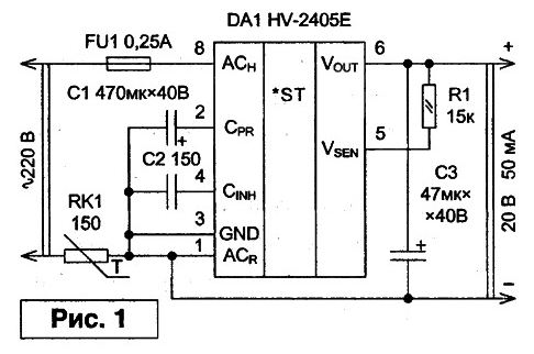
The device is made of only seven components, and plays a major role a specialized chip HV-2405E firm "Harris Semiconductor" [1, p. 25-31]. Functionally chip HV-E consists of two systems -advanced switching regulator and terminal linear regulator voltage. Schematic diagram of the power source, positioned as a model, is shown in Fig. 1. This single-chip power source has not galvanic isolation voltage of input and output circuits, but has a chain protection against short-circuit in the load method of limiting current.
The appointment and replacement of components
The thermistor RK1 prevents the breakdown of circuits DA1 the charge current of the capacitor C1. In the power source used was a small thermistor brand MZ21-N151RM, which can be exchanged for instruments brands MZ21-N101RM, MZ21Р121RM, or MZ21Р181RM similar.
Constructive fuse FU1 feeding protects the network from overload in the event accident. The fuse is made from a piece of copper wire with a diameter of about 0.05 mm.
Electrolytic capacitor C1 during one part of the period of the mains tension accumulates energy, and during the other part of the period accumulated energy nourishes terminal linear voltage regulator. From the capacitance this capacitor depends on the maximum current, which is able to give to the load the power source. The capacitor can be any brand and manufacturer, but definitely small.
Ceramic capacitor C2 provides a delay enable circuits DA1 in during time duration transients. For mains frequency in 50 Hz or 60 Hz recommended capacitance of the capacitor 150 pF. The capacitor C2 can be applied with any type nominal voltage of 40 V. Bosminidae DA1 chip encased in a standard DIP-8, provides converting the AC input voltage to DC output voltage and is designed to stabilize the latter. Operating temperature range of the chip HV3-2405E-5 is 0°C… +75°C, and the chip HV3-2405E-9 reaches -40°C … +85°C. the Crystal chip can be heated to a temperature of +150°C.
The purpose of the pins is as follows:
Electrolytic capacitor C3 performs the function of a capacitive filter, smoothing the ripple of the output voltage of the power source. The more its capacity, the will be less output voltage ripple.
The resistance of the resistor R1 included in the feedback circuit determines the value of DC output voltage. A resistor can be used brand MLT, S2-22, C2-23 or equivalent. The magnitude of the current flowing through the resistor, approximately 1 mA.
Design
Installation of the power source can be made in hinged manner. To the radio components to be soldered conclusions dliii at least 10 cm of flexible the wires in high-quality insulation, which should be oriented in the same direction. Mark the wire can be, for example, MGTF. The wires should be tinned and to mark them, that there was no further question concerning their connection with components of the power supply. After Assembly and confirm the performance of the the product is dipped in epoxy compound and several layers envelop fiberglass. Then the workpiece is placed inside a specially prepared metal sewing thimble so that the flexible findings came from him. The thimble performs the functions of the housing and an electromagnetic shield. Finally pour the contents of the thimble epoxy compound so that the fiberglass is completely covered by the polymer. For to release air bubbles, a thimble carefully shake.
By the end of the day the compound will harden, and the power source can be used for the purpose intended. It should be noted that after pouring the thimble power source will not be maintainable. That is, all adjustment operations must be conducted before assembling products in a single unit.
Setup and adjustment
The power source does not require an adjustment, if made in precise accordance with the concept and made of non-defective parts. In the case of the need to adjust the output voltage should change the resistance resistor R1. Thus, to obtain the output voltage value 18 In the resistance of the resistor R1 must be 13 ohms, 15 - 10K,for 12 In - 6,8 kOhm, and 9 In - 3,9 kOhm.
Literature
Author: Eugene Moscato Taganrog, http://moskatov.narod.ru