


")

Creating a stereo amplifier for the stereo system or, as they say, home theatre, modern integral element base, we want the source power kept pace with progress. Moreover, the switching power supply not only interesting from the point of view of progress, but also practical. After all, to find a suitable power transformer, or only the core with the shell, it is now difficult, and if there was a suitable subject, it will be very bulky and heavy.
Searched a bit on the Internet, looked through the Datasheet and service manuals for TV, and that's what happened diagram shown in the figure.
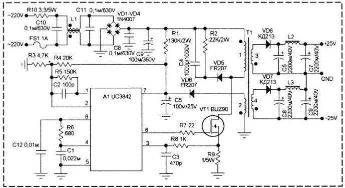
Circuit is a flyback switching power supply based on the IC UC3842 PWM. The scheme is almost typical, almost like recommends the manufacturer of this IC.
The voltage from the mains via a throttle filter C10-L1-C11 is supplied to bridge rectifier diodes VD1-VD4. Resistor R10 limits the impulse inrush current the charging of the capacitor C9. The DC voltage at the output this rectifier is about 300 V.
Power to the chip A1 is supplied in two ways. Inrush power through R1. After run the generator power begins to flow from the winding 2 of the transformer T1 through the rectifier diode VD6. This same voltage and control is for the circuit voltage (control circuit voltage flows through R3-R5-C2).
The generated pulses are received from the A1 pin 6 to the gate of the field-effect transistor VT1 In its stock chain included primary winding of pulse transformer T1. In the source circuit of the resistor R9, which is used for the protection circuit of this transistor from over-current. When exceeding the permissible current, the voltage at this resistor increases and is supplied to the control input A1 (pin 3). If the voltage on this pin exceeds the threshold value - output stage off (no longer receive the pulses VT1).
The secondary voltage ±25 V formed by two independent secondary windings 3 and 4, and accordingly rectifiers diode VD7 VD6 and. Then, DC current, they are connected in series. If the amplifier circuit requires a separate sources of non-point GND, then they can disconnect.
Output voltage 2x15, when the load current 2x2 A.
Despite the presence of a stabilization in the primary circuit, the secondary voltage unstable. Rather, their value is not changed when you change network voltage over a wide range, but is subject to some changes based from the load. Almost as depending on the load change the output voltage rectifier fed from a conventional low frequency power transformer.
I have the power stereo amplifier works with chips TDA2030 (without additional transistor "mosnita") in the schema of the MIND, with the output power 2x15 watts.
As the core and the armature to the pulse transformer is used the frame and core pulse transformer TV 3-USCT. Primary winding of the transformer T1 (1) contains 60 turns of wire sew 0,61. Winding 2-10 of turns of wire sew 0,43 windings 3 and 4 through 10 turns of wire sew 0,61. Winding all coils need to perform as indicated in the diagram (start winding marked bold dots), the direction of all of the windings are the same.
Choke L1 - ready choke mains filter from the same TV. Chokes L2 and L3 are wound on a ferrite rings outside diameter of about 20 mm, it contain 20 turns of wire sew 0,61.
The transistor needs a radiator.
In the process of building can be made clear that the output voltages are different from a settlement. Then they can be customized a bit to the desired value by selection of the resistance R4. This resistor be replaced only after the power supply switch off from the mains. The increase R4 leads to an increase in voltage and a decrease causes a decrease in the output voltage.
Author: P. F. Gardeners