


")

Often collecting any electronic design, such as: the audio frequency amplifier, automation equipment, devices based on microcontrollers, and more, we wonder what to supply the equipment? Electronic devices mostly feed on a constant voltage different from the supply voltage. In recent years, increasingly pulse technique displaces from daily use traditional transformer circuits of power supplies. The win here is obvious, firstly it saves winding material, which is not cheap. Second, there is the size and weight of the devices, nowadays, with modern miniaturization of the apparatus for various purposes, this question is very relevant, most schemes UPS quite difficult to build and configuration and is not available to repeat novice Amateurs.
This article provides a simple scheme of the UPS, the aim was simplicity, good repeatability, the use of the material at hand, not the complexity of the Assembly and setup. Despite the simplicity, the UPS has a pretty good performance.
Specifications
Supply voltage: 220 V/50 Hz.
Rated output power: 300 W
Maximum output power: up to 500 W
The frequency of the voltage conversion: 30 kHz
Secondary rectified voltage varies as needed
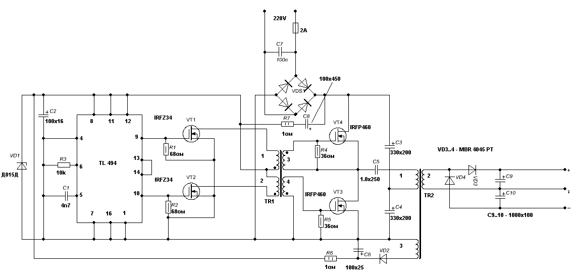
Schematic diagram
(click to enlarge)
The principle of operation of the UPS is as follows: pulses to control the master oscillator generates built on a special driver TL494, the frequency of the control pulses of 30 kHz. The control pulses from the outputs of the chip are served in turn on the transistor switches VT1,VT2 preliminary pulse shaper output power keys. The keys VT1,VT2 loaded with control transformer TR1, and which forms the control pulses of powerful output keys VT3,VT4 ,driver needed for galvanic isolation gate circuits of the output stage. UPS is built on the half-bridge circuit, the middle point of the half bridge is created by capacitors C3,C4, which also serves as a smoothing filter is rectified by a diode bridge supply voltage VDS1 of the network.
The circuit R7,C8 provides short-term power to the master oscillator and pulse shaper control for initial startup of the UPS, after a full charge the capacitor C8 power to the driver is performed directly by the winding 3 of the transformer TR2 c which removed the AC voltage of 12V. Chain VD2 ,C6 is used for straightening and smoothing the supply driver voltage. The Zener diode limits voltage VD1 initial startup to 12V.The secondary voltage supply for the electronic equipment is removed from the winding 3 of the transformer TR2, rectified by diodes Schottky VD3, VD4 and is fed to a smoothing filter C9,C10. If the voltage exceeds 35V, includes two diodes in series.
A few words about the design of the UPS: most of the components are taken from faulty computer PSU ATX. Namely, this chip TL494, capacitors C9,C10, a diode bridge VDS1, capacitors C1,C2, C5,C6,C7, diode VD2, diodes Schottky VD3,VD4, and a ferrite core frames TR1,TR2.
The UPS itself was structurally assembled in the case of the same disassembled the ATX PSU transistors VT3,VT4 installed on the radiator area 50cm/sq
Data rewind transformers TR1,TR2:
TR1, all four coils contain 50 turns of wire 0.5 mm
TR2, the Winding 1 is wound wire 0.8 mm 110 turns. 3 comprises a winding 12 of turns of wire 0.8 mm. Winding 2 is wound depending on the required secondary voltage and is calculated from the ratio Vit./Volta. Since the output is a voltage doubler.
Success in repetition!
Download the printed circuit Board in the format Layot (6 KB)
Author: Arthur (left-handed); Publication: www.cxem.net