


")

To improve the performance of switching power supplies are collected on the basis of bridge and half-bridge converters, in particular, to reduce the likelihood of the occurrence of a through current and increase the efficiency, the authors propose to translate such sources in quasi-resonant mode of operation. In this article practical example of such a power supply.
Often to reduce the size and weight of power sources (IP) network transformer replace pulse transformers. The gains from this are obvious: smaller weight and dimensions substantially less consumption of copper for coilers, high efficiency IE. However, pulse SP has its drawbacks: bad electromagnetic compatibility, possibility of occurrence of a through current through the transistors in push-pull converters, the need for the introduction of chains protection against overcurrent, the complexity of the launch of the capacitive load without the adoption of special measures to limit the charging current.
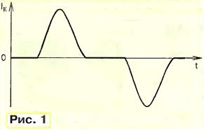
Consider the example of half-bridge push-pull self voltage Converter [1], as to some extent it is possible to exclude or to reduce these disadvantages by changing the mode of its operation. Translate Converter in quasi-resonant mode of operation by entering the resonant circuit [2]. The form of the current through the primary winding of pulse transformer in this case is shown in Fig. 1.
In Fig. 2 shows the shape of voltage and current for one of the switching the transistors. The figures show that the Converter operates in quasi-resonant mode - through current in this case is absent.
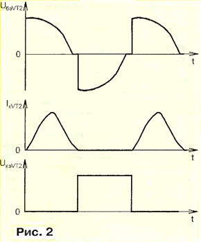
The voltage at the base of the switching transistor is reduced and the end of pulse becomes zero. Thus, the transition to the quasi-resonant mode eliminates dynamic switching losses in the transistors and problems associated with electromagnetic compatibility sensitive devices with pulse IE, because the spectrum of the generated oscillations is sharply narrowed.
Half-bridge Converter differs from two-stroke overhead fewer the used transistors; from two-stroke with an average o - lower half the voltage on the transistors. Self Converter differs from converters with a master oscillator, first and foremost, a minimum number elements, the maximum possible efficiency, and the use of saturated auxiliary transformer is guaranteed to eliminate any possibility of through current.
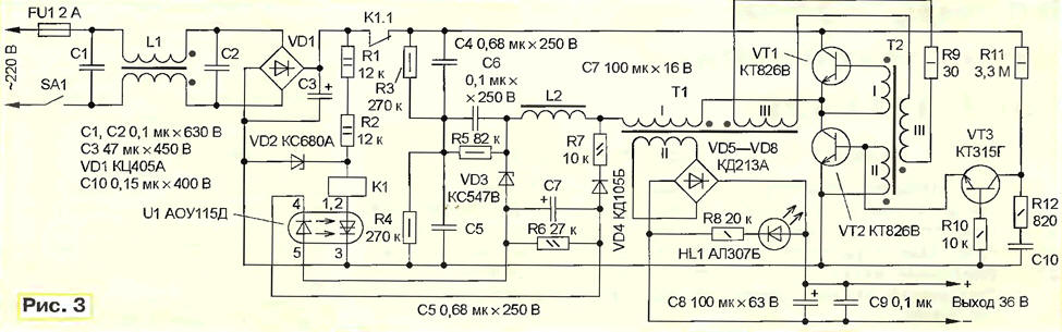
Diagram of half-bridge quasi-resonant IC, devoid of these drawbacks, it is shown in Fig. 3.
(click to enlarge)
Main technical characteristics
- Interval changes in supply voltage, ....198…264
- Maximum efficiency, %......92
- Output voltage, V, load resistance of 36 Ohms......36
- The working distance of converting frequency, kHz......12 57…
- The maximum output power, W......70
- The maximum amplitude of the output ripple voltage with an operating frequency, In......2,2
IE contains the following nodes: noise filter С1C2L1 that prevents penetration into the supply line of the high-frequency pulsations, generated by the transducer; a network rectifier VD1 with filter capacitor C3; a protection circuit against overload and short circuits in the load R1R2VD2K1U1VD3VD4R6R7C7. The protection circuit consumes little current, so little affects the overall efficiency of the source, but if necessary, the efficiency can be somewhat be increased by replacing the Zener diode VD2 more high voltage. Resistors R6 and R7 form a voltage divider that is required to enable emitting diode triac optocouplers. If these fixed resistors to replace one variable, in a very wide range to adjust the threshold. If it is expected to supply the load with large capacity (more than 5000 µf), for eliminate false positives protection should increase the capacitance of the capacitor C7, however, the waiting time until the power supply is turned on in this case will increase.
Elements R3, R4, C4, C5 form a voltage divider. Resistors R3, R4 necessary to discharge the filter capacitors C3 and divider after SS turn off the power supply. The capacitor C6 and the inductor L2 of the resonant circuit. The triggering circuit is exactly the same as in the device described in the article [1]. She consists of transistor VT3, resistors R10-R12 and capacitor C10. Transistor VT3 is working in avalanche mode. Pulse opens the transistor VT2, providing initial asymmetry.
Diodes VD5-VD8 - output rectifier filter capacitors C8, C9. HL1 led indicates presence of voltage at the output of a PI. Auto generation oscillation occurs as a result of positive feedback the winding III of the transformer T1 to the winding III of transformer T2 through current limiting resistor R9. Decreasing the resistance frequency conversion is reduced, which leads to a shift of the maximum of the efficiency of the source in the direction more power to the load.
The device incorporates capacitors K73-17 (C1, C2, C6, C9, C10), K73-11 (C4, C5), C50-32 (C3), C50-24 (C7, C8). All resistors - C2-23. Instead, these capacitors and resistors may use other components, however, capacitors should be chosen with a minimum tangent of dielectric losses in the working frequency interval of conversion.
Diode bridge VD1 - anyone with a valid direct current of 1 A and a valid reverse voltage of at least 400 V, for example BR310. It is possible to use discrete diodes, for example KDR connected in a bridge circuit. In the device it is best to use a transistor CTG (VT3) - this starts the chain will be to work immediately, the transistor KT315B have to pick up, and the transistors CTA, CTV better not to apply. Transistors CTV (VT1, VT2) any of the interchangeable series CT or CTA, CTB. Due to small losses of the transistors can not to install the heat sinks. The output rectifier diodes KDA (VD5-VD8) it is permissible to replace CDB, CDU or series CD, CD. They should be installed on a heat sink with a cooling surface area of not less than 10 cm2.
In SP applied electromagnetic relay DC GBR10.1-11.24 working 24 volt, capable of switching AC 8 And in circuits with voltage up to 250 V. It can be replaced with any other valid dial-up an alternating current of 1 A in circuits with voltage of 250 V. However, it is desirable to use relays with a minimum current to improve the efficiency of the power supply unit, because less than the trip current, the greater the resistance must have resistors R1, R2, and less power will be dissipated.
Inductors L1, L2 and transformer T1 is used to finish - from the old computing machine IS: L1 - 5, L2 - 4777026 or 009-01, T1 - 052-02. Their can be made independently. The inductor L1 is wound (two winding) on the annular magnetic core Chg ferrite (for example, brands MNM or MNM-17) or alsever. Windings contain 315 turns the PEV-2 to 0.3.
The resonant inductor L2 is wound on an annular magnetic core from Khh ferrite MNM-A. Its winding contains 13 turns of wire sew-2 of 0.6.
The transformer T1 is wound on the annular magnetic ferrite CHH MNM-17. Winding I has 200 turns of wire sew-2 0,6, winding II - 35 turns of PEV-1 2, winding III - 5 turns of wire sew-2 of 0.6. Order winding the windings on the magnetic core is arbitrary. Between the windings must lay the insulation layer, for example, PTFE tape. In addition, the transformer should be impregnated, for example, from paraffin candles or ceresin. This will not only increase the electrical strength of the insulation, but will also reduce the hum, generated by the source at idle.
Transformer T2 is wound on the annular magnetic ferrite CHH MNM-A. Windings I and II contain seven turns of wire sew-2 0,3 ( wound simultaneously in two wires), and winding III - nine turns of wire Sew-2 to 0.3.
Design of IE can be arbitrary, the relative position of the elements on the Board not critical. It is only important to provide a good flow of air to the semiconductor devices by natural convection or install IE inside the powered device near the fan.
In establishing described Yip almost not necessary, although you should ensure that the Converter operates in quasi-resonant mode. For this purpose, the output of the block power connect the dummy load resistor 100 watts and the resistance of 36 Ohms. In series with the capacitor C6 include additional resistor 0,1… 1 Ohm and power 1…2 watts. Additional the resistor connect the oscilloscope probes: General - to the midpoint of the divider voltage R3R4C4C5, signal to the capacitor C6. You must ensure that the oscilloscope is not galvanically connected to the network. If connected, to the network should to connect via an isolation transformer with a transformation ratio of 1:1. In any case, you must observe the safety rules. By submitting nutrition on IE, assured that there is a bell-shaped current pulses with a pause at zero. If the pulse shape is different from that shown in Fig. 1, it is necessary to choose the number of turns of the inductor L2 to produce resonance.
For extra resistor 0.1 Ohm pulse amplitude should to be about 0.1 V. Now you should compare the shape of the current and voltage at a switching transistor VT2 from the one shown in Fig. 2 graphs. If they similar in shape, IP operates in quasi-resonant mode.
The threshold can be changed. For this selected resistance resistor R7 so that the protection is triggered when the required load current. If it is necessary that PI unplugged with power in the load is less than 70 W, the resistance of the resistor R7 should be reduced.
To limit the charging current of the capacitor C3 at the time of inclusion we recommend you to break any of the connecting cord to connect the resistor 5,6… 10 Ohm 2W power.
Literature
Authors: Y. Haino, E. Maskaev, Taganrog, Rostov region