


")

Give a complete description of circuit diagram for one of the 200-watt switching power supply units (PS6220C, production Taiwan).
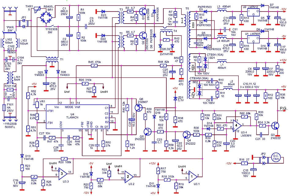
Alternating voltage is supplied through the power switch PWR SW through mains fuse F101 4A, spike filters are formed elements S, R101, L101, S, C103, C102 and chokes L102, L103 on:
- output three-pin connector, which can podstegivaniia cable power display;
- two-pin connector JP1, second part is on Board.
Connector JP1 AC voltage supplied to:
- bridge rectification circuit ВR1 via thermistor THR1;
- the primary winding of the starting transformer T1.
The output of the rectifier ВR1 included a smoothing capacitance filter C1, C2. The thermistor THR initial limits the throw of the charging current of these the capacitors. Switch 115V/230V SW enables power-UPS as from 220-240 V, and from the network 110/127 V.
Vysokoumnye resistors R1, R2, shunt capacitors C1, C2 are balun (equalize the voltages on C1 and C2), as well as provide the discharge of these capacitors after UPS shutdown from the network. The result of the work input circuits is the appearance of the rectified bus voltage DC voltage Uep equal to +310, with some ripple. This UPS has used a scheme run with forced external excitation, which implemented on a special pad transformer T1, the secondary winding of the after the UPS is turned on in the network, you receive an alternating voltage with a frequency of supply network. This voltage is rectified by diodes D25, D26, which form with a secondary winding T1 a full-wave rectification circuit with a medium point. C30 - a smoothing filter capacity, which produces a constant voltage, used to power management chip U4.
As the control chip this UPS is traditionally used IC TL494.
The supply voltage from the capacitor C30 is supplied to the terminal 12 U4. As a result the output 14 U4 appears the output voltage internal reference source Uref=-5 In, starts an internal sawtooth generator circuits, and conclusions 8 and 11 appear control voltages which are sequence of rectangular pulses with a negative front edges, shifted relative to each other by half of the period. Elements S, R50, connected to the terminals 5 and 6 of chip U4 determine the frequency of the sawtooth the voltage generated by the internal clock of the chip.
A matching stage this UPS made by betransitory scheme with separate control. The voltage of the capacitor C30 is served at the midpoints the primary windings of the transformers T2, T3. The output transistors IC U4 perform the function of matching transistors of the cascade and connected in the circuit with the MA. The emitters of both transistors (pins 9 and 10 of the chip) is connected to the "body". The collector loads of these transistors are the primary Polubotko governing transformers T2, T3, connected to the terminals 8, 11 chips U4 (open collectors of the output transistors). The other half of the primary windings T2, T3 connected diodes D22, D23 form a degaussing circuit the cores of these transformers.
Transformers T2, T3 control a half-bridge power transistors of the inverter.
Switching of the output transistors of the chip cause the appearance of a pulse governing the EMF in the secondary windings of the transformers T2, T3. Under the EMF of the power transistors Q1, Q2 are alternately opened with adjustable pauses ("dead zones"). Therefore, through the primary winding power pulse transformer T5, an alternating current in the form of sawtooth current pulses. This is because the primary winding of T5 included in the diagonal of the electric bridge, one shoulder which is formed transistors Q1, Q2, and the other capacitors C1, C2. Therefore, when opening any of the transistors Q1, Q2 primary winding of T5 is connected to one of the capacitors C1 or C2, which causes the flow of current during the entire time that open the transistor.
Damper diodes D1, D2 serve to return the energy stored in the inductance scattering of the primary winding of T5 during a closed state of the transistors Q1, Q2 back to the source (recuperation).
Chain C4, R7, shunting the primary winding of T5, inhibits high-frequency parasitic oscillation processes that occur in the circuit, formed by the inductance of the primary winding of T5 and its inter-turn capacity when the closing of the transistors Q1, Q2, when the current through the primary winding sharply ceases.
Capacitor C3, connected in series with the primary winding of T5, eliminates constant component of the current through the primary winding of T5, thereby eliminating the unwanted magnetization of its core.
Resistors R3, R4 and R5, R6 form the basic factors for a high-power transistors Q1, Q2 respectively and provide optimal mode switching from the point the dynamic view of power losses on these transistors.
The flow of alternating current through the primary winding of T5 leads to the existence of alternating rectangular pulse EMF in the secondary windings of this of the transformer.
Power transformer T5 has three secondary windings, each of which has the output from the midpoint.
Winding IV provides receiving the output voltage +5 V. Diode Assembly SD2 (half-bridge) forms a winding IV the full-wave rectification circuit with an average point (mid-point grounded winding IV).
The elements L2, C10, C11, C12 form a smoothing filter in the channel +5 V suppression of parasitic high-frequency oscillatory processes that occur when switching diode Assembly SD2, these diodes are shunted soothing RC-chain C8, R10 and R9, R11.
Diodes Assembly SD2 are diodes with Schottky barrier than is achieved the high performance and increases the efficiency of the rectifier.
Winding III together with the winding IV provides receiving the output voltage +12 V with diode Assembly (half-bridge) SD1. This Assembly forms a winding III the full-wave rectification circuit with a medium point. However, the mid-point the winding III is not grounded, and connected to the bus output voltage +5 V. This will give you the opportunity to use Schottky diodes in the channel generate +12V, because reverse the voltage applied to the rectifier diodes with this inclusion, reduced to acceptable for Schottky diodes.
Elements L1, C6, C7 form a smoothing filter in the channel +12 V.
Resistors R9, R12 are designed to accelerate the discharge of the output capacitors tire +5 V and +12 V after UPS shutdown from the network.
RC-chain C5, R8 is designed to suppress oscillatory processes, occurs in the parasitic circuit formed by coil inductance and III inter-turn capacitance.
Winding II with five taps provides a negative output voltage -5 V and -12 V.
Two discrete diode D3, and D4 form a half-bridge full-wave rectification in the channel for developing -12 V, and diodes D5, D6 - channel -5 V.
Elements L3, and L2 C14, C12 form a smoothing filters for these channels.
Winding II and III winding, shunted sedative RC-chain R13, C13.
Mid-point of the winding II is grounded.
Stabilization of the output voltage are carried out in different ways in different the channels.
Negative output voltage -5 V and -12 V are stabilized by the linear three-terminal integrated stabilizers U4 (type 7905) and U2 (type 7912).
For this purpose, the inputs of these stabilizers are output voltage rectifiers with capacitors C14, C15. On the output capacitors C16, C17 succeed stabilized output voltage -12 V and -5 V.
Diodes D7, D9 provide discharge of the output capacitors C16, C17 through resistors R14, R15 after UPS shutdown from the network. Otherwise these capacitors discharged through the scheme stabilizers, which is undesirable.
Through resistors R14, R15 and discharged capacitors C14, C15.
Diodes D5, D10 serve a protective function in case of breakdown of the rectifier diodes.
If at least one of these diodes (D3, D4, D5 or D6) will be "punched", the absence of diodes D5, D10 to the entrance of the integral stabilizer U1 (or U2) applied positive pulse voltage, and through an electrolytic capacitors C14 or C15 have proceeded alternating current, which would lead them to the exit out of action.
The presence of diodes D5, D10 in this case eliminates the possibility of such situation, because the current is closed through them.
For example, in the case that pierced through the diode D3, the positive part of the period when D3 should be closed, current will close the circuit:-D3 - L3 D7-D5- "body".
Stabilization of the output voltage +5 V is performed by the PWM method. For this to the bus output voltage +5 V connected measuring resistive divider R51, R52. The signal proportional to the output voltage in the channel, +5 V, is removed from the resistor R51 and is fed to the inverting input of the error amplifier DA3 (output 1 control chip). The direct input of the amplifier (pin 2) served reference level voltage from the resistor R48 included in the divider VR1, R49, R48, which is connected to the output of the internal reference source of chip U4 Uref=+5 V. When the level changes in bus voltage +5 V under the influence of various destabilizing factors there is a change the magnitude of the error (error) between the reference and controlled levels the voltage at the inputs of the error amplifier DA3. As a result, the width (duration) the control pulses of the pins 8 and 11 of chip U4 is changed so that to return runaway output voltage +5 V to the nominal value of (if you reduce bus voltage +5 In the width of the control pulses increases, and increasing the voltage decreases).
Sustainable (without the occurrence of parasitic oscillation) the entire loop regulation is achieved by a chain of frequency-dependent negative feedback covering the error amplifier DA3. This chain is inserted between the conclusions 3 and 2 control chip U4 (R47, S).
Output voltage +12 V in this UPS is not stabilized.
Adjusts the output voltage in this UPS is only for the +5 V and +12 V. This adjustment is performed by changing the level the reference voltage on the direct input of the error amplifier DA3 using trim resistor VR1.
When the position of the engine VR1 in the process of setting up the UPS will change certain limits the voltage level on the bus +5 V, and hence on the +12V rail, because the voltage bus +5 V is supplied to the midpoint of the winding III.
Combined sewn for the UPS includes:
- limiting the control width of the control pulses;
- full circuit protection short circuit in the load;
- incomplete monitoring circuitry output over-voltage (only on the bus +5 V).
Let us consider each of these schemes.
Limiting the control scheme uses as a sensor current transformer T4, whose primary winding is connected in series with the primary winding power pulse transformer T5.
The resistor R42 is the load of the secondary winding T4 and diodes D20, D21 form the full-wave rectification circuit, the alternating pulse voltage, remove from the load R42.
Resistors R59, R51 form a divider. Part of the voltage is smoothed capacitor C25. The voltage on this capacitor is proportional to depends on the width of the control pulses at the bases of the power transistors Q1, Q2. This level through resistor R44 is fed to the inverting input of error amplifier DA4 (pin 15 of chip U4). Direct input of the amplifier (pin 16) is grounded. The diodes D20, D21 are included so that the capacitor C25 current flow through these diodes charged to a negative (relative to the common wire) voltage.
In normal operation, when the width of the control pulses does not go within the permissible limits, the potential of the pin 15 is positive, due to the connection of this output through a resistor R45 to the bus Uref. When excessive increase in the width of the control pulses for any reason, the negative voltage on the capacitor C25 is increasing, and the potential of the pin 15 becomes negative. It leads to the appearance of the output voltage of the error amplifier DA4 that was equal to 0 V. Further increase of the width of the control pulses causes the switching control PWM comparator DA2 is transmitted to the amplifier DA4, and the subsequent increase in width of the control pulses is not happening (private mode), because the width of these pulses ceases to depend on the level the feedback signal to the direct input of the error amplifier DA3.
Protection circuitry against short-circuit in the load can be conditionally divided into the protection channels provide positive voltages and protection channels creating a negative stress, as for the circuit, which is implemented in roughly the same way.
Sensor circuits short circuit protection in load channels to provide positive voltages (+5 V and +12 V) is the diode-resistor divider D11, R17, connected between the output tires these channels. The voltage level at the anode diode D11 is controlled signal. In normal operation, when the voltage on output buses the +5 V and +12 V are of nominal value, the anode potential of the diode D11 is about +5.8 V, because through the divider-sensor current flows from the bus +12 V bus +5 V circuit: bus +12 V - R17-D11 - bus +5 V.
The monitored signal from the anode of D11 is supplied to the resistive divider R18, R19. Part of the stress is taken off the resistor R19 and served on a direct entry comparator 1 chip U3 type LM339N. The inverting input of comparator served reference level voltage with resistor R27 divider R26, R27, connected to the output of the reference source Uref=+5 V control chip U4. Reference level is selected such that during normal operation, the potential direct input of the comparator 1 would exceed the potential of the inverted input. Then the output transistor of the comparator 1 is closed, and the UPS circuit normally operates in PWM mode.
In the case of a short circuit in the load channel +12 V, for example, the anode potential of the diode D11 becomes equal to O, so the potential of the inverting input of the comparator 1 becomes higher than the potential of direct input, and the output transistor of the comparator will open. This will cause the closing of the transistor Q4, which is normally open current base passing through the circuit: bus Upom - R39 - R36 b-e Q4 - "body".
The opening of the output transistor of the comparator 1 connects a resistor R39 to "the body", and therefore, the transistor Q4 passively closes a zero offset. The closing of the transistor Q4 entails charging the capacitor C22, which performs the function of link delay protection operation. The delay required from those considerations that in the process of UPS output mode, the output bus bar voltage +5 V and +12 V do not appear immediately, and as the charging of the output capacitors large capacity. Reference same voltage source Uref, by contrast, appears almost immediately after turning on the UPS to the network. Therefore, in the starting mode the comparator 1 is switched, the output transistor is open, and if check the capacitor C22 was absent, it would have led to actuation of protection immediately when you turn on the UPS to the network. However, the scheme includes C22, and this protection is only after the voltage across it reaches level determined by the resistors R37, R58 divider connected to bus and Upom which is the base for the transistor Q5. When this happens, the transistor Q5 is opened and the resistor R30 is connected through a small the internal resistance of this transistor to "body". So there is a path for the flow of the base current of the transistor Q6 through the circuit: Uref - e-b Q6 - R30 - to-e Q5 "the corps".
Transistor Q6 opens this current to saturation, resulting in the voltage Uref=5 V, which is supplied by the emitter of the transistor Q6, is applied through its small internal resistance to pin 4 of the management of chip U4. This, as previously shown, leads to stop the operation of the digital path chip, the loss of output control pulses and the termination switch power transistors Q1, Q2, i.e. protective shutdown. Short circuit in the load channel +5V will cause the anode potential of the diode D11 will be only about +0.8 V. Therefore, the output transistor of the comparator (1) will be opened, and happens protective shutdown.
Similarly built short circuit protection in load generation channels a negative voltage (-5 V and -12 V) on the comparator 2 of the chip U3. Elements D12, R20 form diagnosticity divider sensor connected between output tires channels generate negative voltages. Controlled signal is the potential of the cathode of the diode D12. Short-circuit in the load channel -5 In / -12 V, the potential of the cathode of D12 increases (from -5,8 to 0 In a short-circuit in the load channel -12 and up to -0,8 In short-circuit in the load channel -5 V). In any of these cases open normally closed output transistor of the comparator 2, and causes the actuation of protection according to the above mechanism. Thus reference level with resistor R27 is fed to the direct input of the comparator 2, and the potential of the inverting input is determined by the resistors R22, R21. These the resistors form a bipolar powered divider (resistor R22 connected to the bus Uref=+5 V, and the resistor R21 to the cathode of the diode D12, the potential of which in normal the mode of operation of the UPS, as already noted, is -5,8 In). Therefore, the potential an inverting input of the comparator 2 in normal mode supported lower than the potential of direct input, and the output transistor of the comparator will be closed.
Protection against output over-voltage on the bus +5 V is implemented on the elements ZD1, D19, R38, C23. The Zener diode ZD1 (with breakdown voltage of 5.1 In) connects to the bus output voltage +5 V. Therefore, while the voltage on the bus is not exceeds +5.1 V, the Zener diode is closed, and closed the transistor Q5. In the case of increasing bus voltage +5 V above +5.1 V Zener diode "breaks", and in the base of transistor Q5 flows gate trigger current, which leads to the opening of the transistor Q6 and voltage Uref=+5 V at pin 4 of the management of chip U4, ie protective shutdown. Resistor R38 is the ballast for the Zener diode ZD1. The capacitor C23 prevents tripping of protection in case of accidental short emission bus voltage +5 V (for example, due to the setting voltage after an abrupt decrease of the load current). The diode D19 is decoupling.
Diagram of the signal PG this UPS is isolated and collected the Comparators (3) and (4) of the chip U3 and the transistor Q3.
The scheme is based on the principle of controlling the presence of a low-frequency alternating the voltage on the secondary winding of the starting transformer T1, which acts on this winding only in the presence of the supply voltage on the primary winding of T1. i.e. while the UPS is plugged in the mains.
Almost immediately after switching on the UPS to the mains supply appears auxiliary voltage Upom on the capacitor C30, which is supplied with the control chip U4 and auxiliary chip U3. In addition, an alternating voltage with the secondary winding of the starting transformer T1 through the diode D13 and current limiting resistor R23 charges the capacitor C19. Voltage with C19 powered resistive divider R24, R25. With resistor R25 part of this voltage is supplied to the direct input of the comparator 3, which leads to the closing of his the output transistor. Appearing immediately after the output voltage the internal reference source chip U4 Uref=+5V feeds the divider R26, R27. Therefore, the inverting input of the comparator 3 is fed a reference level with resistor R27. However, this level is selected to be lower than the level of the direct input, and therefore, the output transistor of the comparator 3 is in the closed state. So begins the charging process of the inhibiting capacity C20 chain: Upom - R39 - R30 - C20 - "body".
Increasing the extent of charging of the capacitor C20 voltage is applied to the inverted input 4 of the chip U3. The direct input of the comparator with a voltage supplied resistor divider R32 R31, R32 connected to the bus Upom. Until the voltage on charging the capacitor C20 does not exceed the voltage on the resistor R32, the output the transistor of the comparator 4 is closed. Therefore, in the base of the transistor Q3 flows opening the current circuit: Upom - R33 - R34 - b-e Q3 - "body".
The transistor Q3 is open to saturation, and the PG signal taken from its collector, has a passive low and blocks the running CPU. During this time, in during which the voltage level on the capacitor C20 reaches the level at the resistor R32, the UPS is securely manages to get in nominalne mode of operation, i.e. all its output voltage in full.
As soon as the voltage exceeds C20 voltage taken from R32, the comparator 4 switches, and the output transistor is open. This will entail the closing of the transistor Q3, and the PG signal taken from its collector load R35, becomes active (H-level) and allows execution of the processor.
When you shut down the UPS from the network to the secondary winding of the starting transformer T1 AC voltage disappears. Therefore, the voltage on the capacitor C19 quickly decreases due to the small capacity of the latter (1uf).
As soon as the voltage drop across the resistor R25 is less than the resistor R27, the comparator 3 switches, and the output transistor is open. It entail safety shutdown output voltages of the flow chip U4, because this opens the transistor Q4. In addition, through the open output transistor comparator 3 will begin the process of rapid discharge of the capacitor C20 through the circuit: (+)C20 - R61 - D14 - to-e of the output transistor of the comparator 3 is "body". As only the voltage level on C20 becomes less than the voltage level at R32, the comparator 4 switches, and the output transistor is closed. This would imply an opening of the transistor Q3 and the transition of the PG signal in an inactive low level before you begin it is unacceptable to decrease the voltage on output buses UPS. This will lead to the initialization signal system reset the PC to its original as all digital parts of the computer.
Both of the comparator 3 and 4 are diagrams generation signal PG covered by positive feedback through resistors R28 and R60, respectively, accelerating their the switching.
Smooth transition to a regime this UPS has traditionally provided by forming chain C24, R41, is connected to pin 4 of the management of chip U4. Residual voltage on pin 4, which determines the maximum possible the duration of the output pulses is set by the divider R49, R41.
The power to the fan motor is energized with capacitor C14 in the channel for developing a voltage -12 V through additional decoupling the l-shaped the filter R16, C15.
Authors: A. V. Golovkov, V. B. Lubitsky