


")

This scheme switching power supply with half-bridge Converter with regulated output voltage without stabilization is used to power the soldering station. The construction and commissioning of this power supply does not cause difficulties, what is the main advantage. The control unit is made on chip CREW, which is a high frequency. PWM controller, to build optimized two-stroke high-frequency pulse power sources.
Diagram of the device shown in Fig. 5.23. The voltage supplied to the filter C1, L1, C2, rectified by a diode bridge VD1 and through current limiting resistor R6 charges the capacitors. JV and C12, forming one arm of the bridge. The other shoulder formed by transistors VT1, VT2 In the diagonal of the bridge included the primary winding transformer T2. Field-effect transistors VT1, VT2 alternately open the pulses from the output circuits DA1, and VT2 is managed directly from chips, and VT1 - through transformer T1 serves for galvanic interchanges. In the chain of gates included resistors R8 and R9, together with containers paddles form. A low-pass filter that reduces noise when switching.
Microchip. A PWM controller CREW has two amplifiers (pins 11, 14), designed for significant output current (flowing and flowing): DC - 0.5 A, pulse - to 2 A. is Controlled by a microchip inside generator, whose frequency is set by connecting a resistor to pin 5 and capacitor to pin 6 (R5, C7 in Fig. 5.23). The frequency Converter in this the case selected is 50 kHz.
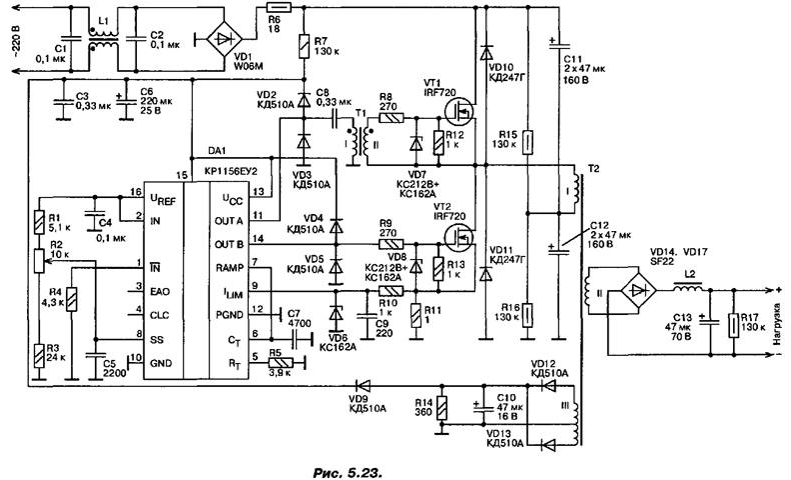
For pulse width modulation of the output signals is used, the device comprising from triggers and error signal amplifier. Using the error signal amplifier it is possible to regulate the output voltage by comparing a part the output voltage with a reference by connecting an appropriately negative feedback to the input of the amplifier. However, in this structure, this feature is not used, so the connections are made as follows. On the non-inverting the input circuit (pin 2) voltage +5.1 V with reference voltage (pin 16). On pin 7 filed sawtooth voltage from pin 6. The inverting input of the amplifier (pin 1) is connected to GND through a resistor R4.
With this inclusion, the error signal amplifier is set to maximum the duration of the output pulses. To control the pulse duration used another possibility controller node "soft start" with the conclusion 8. If this conclusion is to apply varying approximately from 2.25 to 4.5 In voltage, the duration of the output pulses will be regulated in the range 0…100% of max. The maximum pulse duration is, accordingly, 80% of the duration of halftime.
Current on pin 8 is very small (of the order of 10 μa); connecting a capacitor to this the conclusion (it is possible to perform the so-called "soft start", when the work Converter starts with the minimum pulse duration, and gradually, due to the charge of the capacitor increases to a stationary value. In this the device is the pulse duration, and hence the output voltage, adjustable the variable resistor R2. The resistor is included in the chain of divider R1.R3, connected to a reference voltage +5,1 V.
The output destination 9 IC - current protection. If the current through the transistor VT2 exceeds 1 amp, the voltage at pin 9 will be more than 1 V and output circuits switches to the off state before the end of the current cycle. Voltage IC supply goes to pin 15. Separate pins for the power supply (pin 13) and the common wire (pin 12) allows, if necessary, to loosen nutrition powerful output stage, which is the source of interference from the rest of part of the Converter.
The power supply for the chip is supplied from the rectifier diode VD12, and VD13 the capacitor C10. When you switch the device to the network this voltage is missing, therefore, it is necessary to solve the problem of initial start-up. To do this, use a further feature of the chip. If the supply voltage of the chip is less than 9 V, the controller is in off state, the output signals. And I. In no, it consumes a current of 1 mA and shunt capacitors C6, which is charged through a resistor R7.
When reaching a voltage of approximately 9.8 V-chip is enabled. The Converter is started, the winding III of the transformer appears voltage, which is rectified and provides power to the chip during work (about 15 In this device). Pin 15 of the chip has a hysteresis about 0.8 In, so will chip off only when the voltage power below 9 V, the result is a momentary decrease in voltage at pin 15 when you run the chip does not lead to its shutdown.
As already mentioned, the shape of the signal at the outputs A and b (pins 11 and 14, respectively) is an alternating pulses appearing maximum duration of 80% from halftime, therefore, between the closing of one transistor and opening another there is a sufficiently large interval. As a result a time when both transistors are open, excluded, and through currents are absent.
The output voltage from the winding II is rectified by diodes VD14…and through VD17 the inductor L2 is supplied to the capacitor C13 and to the inverter output. The purpose of the inductor L2 is the allocation of the rectified sequence rectangular pulses of a constant component. In the pauses between the pulses the rectified voltage all the rectifier diodes are open, and through them the energy stored in the inductor goes to the load.
In the block used parts for import and domestic production: VD1 - diode the bridge W06M with a reverse voltage of 600 V and a maximum current of 1.5 A; SP, C12 - two parallel connected capacitor 47 µf 160 In Jamicon company; VD14 VD17… - import diodes SF22 with a reverse voltage of 100 V and a maximum current of 2 A; the recovery time is 35 NS. It should be noted that the performance of these diodes much depends on the efficiency and the noise level of the device.
The transformer T1 is wound on the ring CHH,5 ferrite MNM, the number of turns the windings I - 50, II - 40, the wire diameter of 0.15 mm, the transformer T2 is wound on the ring CH,5x7 ferrite MNM, winding I has 160 turns of PEV-1 with a diameter of 0.3 mm, II - 40 turns of the same wire diameter of 0.6 mm, III - 2x15 turns of wire with a diameter of 0.15 mm. Choke L2 is wound on the ring of CHH ferrite MNM with a gap in the ring is 1.5 mm; number of turns, wire diameter a Gap of 0.5 mm. made a hacksaw or angle grinder diamond wheel, clearance for the strength of the glued strip of the PCB.
Transistors mounted on a small heat sinks. VD7, VD8 - two series-connected Zener diode on the total voltage stabilization 18 V. Other parts - model for pulsed sources.
When adjusting the device to the terminals 15 and 10 chips DA1 is connected to the external power supply +12 V and checks for the presence of signals at the outputs A and b, their the form and change the duration of pulses in regulating resistor R2. When need matched resistors R1 and R3 to the desired range regulation.
Further 220 is connected In a voltage of the order of 30 to 40 In without disconnecting source +12 V, and checked the signal at the junction point of transistors, and the formation of the voltages at the output and the capacitor C10. Voltage must be proportionally reduced compared to the stationary regime.
Then removed the source of +12 V and the device can be included in the network of 220 V. In least the specified number of turns of the windings I and III of transformer T2: III - to supply + 15 V, and the winding II is required for the maximum voltage of the source.
Author: A. P. Seman