


")

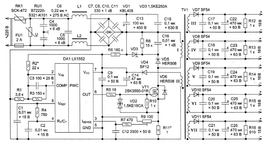
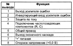
The proposed switching power supply (SMPS) is used to power the master oscillator and four independent, galvanically isolated driver powerful power unit with bridge Converter SMPS performed on the flyback architecture and has a stabilization of the output voltage and protection against overcurrent.
(click to enlarge)
Purpose and possible replacement of components.
The thermistor RK1 (with negative temperature coefficient of resistance) is needed to reduce the inrush current, emerging at the moment of switching SMPS and due to the electrolytic charge capacitor G13. In the scheme used SCK-472 with the initial resistance of 47 Ohms and a maximum operating current of 2 A. It can to change such thermistors B57237-220 S-M (2.8 A, 22 Ohms), B57236-S 250-M (2.5 A, 25 Ohms), B57236-S 800-M (1.6 A, 80 Ohm) or SCK-252R0 (2 A, 25 Ohms); varistor RU1 B72220-S321-K101 data sheets with the voltage 320 To protect the input circuit of the device from overvoltage. You can change the varistors TVR20471, TVR20621, B72214-S301-K, B72214-S321-K101, V-S301-K101 or B72220-S381-K101; fusible fuse FU1 is to protect the mains from the short-circuit current in case of failure of components of the SMPS.
Recommended fuses - IT-2V, NRT-2A/250V or. NRT-2A/250V; the network rectifier assembled the diode VD1 Assembly (LWL408, LWL407, RS407 or RS510) and the capacitive rectifier C13, C15. Capacitor C15 with dielectric polyester bypasses high frequency electrolytic capacitor C13; ceramic capacitor C1 filters the reference voltage V REF; the elements of C2, R4 determine the frequency of pulse generation. By setting the highest value of the operating cycle D and conversion frequency F (in Hertz), empirical formulas can be calculated the resistance R4 (if 0,ЗD0,95) and the capacitance C2:
C3-R3 - chain correction of error signal amplifier, and R1-R2 divider voltages applied to the inverting input of the amplifier error signal; capacitors C4, C5 (Y-class) and C6 (x2-class dielectric polyester type V-S-M or. V-S-M, W-S-M, W-S-M, W-A-M) together with the inductors L1 and L2 form a the filter electromagnetic compatibility, blocking the propagation of pulsation from the SMPS to the mains supply. Inductors L1 and L2 (1.5 mH) is taken brand PLA10AN1522R0R2B manufacturing Murata Manufacturing Co. According to the documentation, these chokes have a nominal voltage of 300 V and a current of 2 A, the capacitors C7, C8, C10 and C11 - ceramic, noise; the controller tracks DA1 fluctuations in the voltage on the capacitors C9 and C14 and by pulse-width regulatory returns attached thereto a voltage to the initial value.
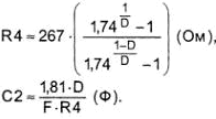
In a result, the constant voltage output of the SMPS is also to some extent stabilize and winding II of the transformer TV1 plays the role of a winding group stabilization. The device uses a specialized the controller LX15521M in DIP-8. Maximum continuous output current terminal of the cascade DA1 - 200 mA, pulsed current is 1 A; a resistor R6 provides initial startup of the master oscillator DA1 (current run - about 250 μa).
The resistance R6 can be calculated by the formula
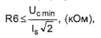
(Uc, min=90 - minimum voltage, ls=250 µa - current run). For stock it is better to take the resistor less resistance; elements VD4 (SF12, to change BYD77D, BYD1100, part no byv27-200, part no sbyv27-200, ES1) C9, C14 form a subsidiary the rectifier pulse-voltage winding II TV1 feeding in DA1 the steady state. The findings VD4 (as иVD7…VD11) need to put ferrite beads, replacing the damping RC-circuit; a resistor R5, included in series with the gate of MOS transistor VT1, reduces high-frequency spurious oscillatory process during switching, the protective diode VD2 (1,CESA, RCES, SMBJ16CA or SMBJ15CA) limits voltage gate-in истокVT1 the time of his charge parasitic capacitance gate-source and gate-drain, and a resistor R10 drains capacitance gate-source VT1 in the pauses of the trigger pulses of the voltage output DA1.
Circuit protection current performed at C12, R7, R9 and R11.
Asyndetically resistor R11 acts as a shunt, which falls a voltage proportional to the current through the source-drain VT1. Trimmer resistor R9 is installed the required sensitivity circuit protection l-shaped filter C12-R7 fixes short spikes that occur at the beginning of the pulse, due to the parasitic parameters key.
Key MOS transistor VT1 - 2SK3550-01R from Fuji Electric (also suitable 2SK3341-01, 2SK3549-01, STW11NK100Z илиSTW12NK90Z). Transistor has a maximum reverse voltage of the source-drain and 900 In the highest permanent the drain current 10 A (pulse - 40 A).
The voltage drop of the source-drain open - 1,08 V. the Transistor is mounted on the cooler HS113-50 (HS151-50) f. Kinstein Co or like landing on a heat-conducting paste. To protect VT1 from breakdown of installed damping chain C16-R8-VD3-VD5. Resistor R8 is asyndetically, carbon. The protective diode VD3 - 1,CEA, can be replaced by 1.CEA, 1.CEA or 1.KEA, and VD5 type HER508 - HFA06TB120 илиHFA06PB120. Diode VD6 - boxer (HER508, UF3010 or UF5408).
Pulse transformer TV1 has a W-shaped magnetic core ETD34 round a core made of a material 3F3 core required non-magnetic gap 0.8 mm. Primary winding I TV1 contains 35 turns sew-2, PETV or petv-2 and wound in a three wire (0.38 mm each), winding II - 6 turns of a single wire of 0.27 mm. Winding III, VI should be, if possible, the same. They are wound in a three wire (0.32 mm) for 6 turns each. Winding VII contains 5 turns and are wound in three wire (0.38 mm).
First a dielectric frame is placed about half turns of the primary winding, laid three layers of insulation from Mylar tape, then placed secondary winding, again winding insulation is laid, and then ends of the winding of the primary winding.
Between the secondary the windings must also be insulation.
After placing all of the windings are wound with several layers of PTFE tape and going to the transformer. Now on top of the windings around all three cores fortified shielding closed loop of copper tape, the edges of which are soldered with each other and are electrically connected with the cathode of the rectifier network.
Ultrafast diode VD7. VD11 brand SF54 straighten impulses arising on the windings III, VII TV1. Data the diodes can be exchanged for BYW29E-150, BYW80-200 or part no mur820.
Ceramic capacitors C17 C21…shunt high frequency electrolytic capacitors C22 C26.... Resistors R12…R16 drain capacitors C17 C26…after turning off the source and, in addition, serve as a loading SMPS.
Used in the power source fixed resistors (capacity up to 2 watts can be brands MLT, ALT, C2-23, P1-4. Ceramic condensators .C3, C9, C12, C17 C21-K10-17, K10-62, K10-73 or equivalent.
Setup and adjustment
First of all the engine tuning resistor R9 put on the far right the diagram position. After checking the installation and futerovok windings TV1 source connected to the network via an incandescent lamp (220 V, 60 W). It protects from SMPS failure in case of errors in the installation or defective parts. If all okay, the lamp is not lit, and the SMPS outputs are continuous voltage. Now, instead of an incandescent lamp in series with the SMPS include ammeter AC measuring limit of 1.2 a, And the outputs of the device connect equivalents loads.
Power SMPS current is not should exceed 0.7 A.
Using an oscilloscope sure on the valve VT1 received impulses rectangular shape with a frequency of about 120 kHz. For accurate billing frequency can slightly pick up the resistance R4 and the capacitance C2. Then checked the output voltages of the SMPS and, if necessary, regulated by selection of the resistance R2.
The final stage - adjustment on the supply voltage using a trim resistor R9, and also check the heating components of the SMPS in a long-term mode.
Author: E. Moscato, Taganrog, Rostov region