


")

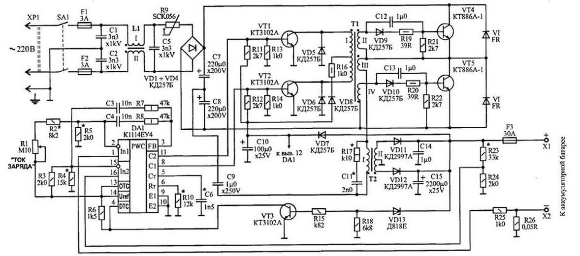
The basis of the device is based on push-pull half-bridge switching Converter (inverter) on a powerful transistors VT4 and VT5, controlled pulse width controller DA1 the low-voltage side. Such converters resistant increasing the supply voltage and the load resistance changes, well proven themselves in the power of modern computers. Because CHI-controllere CEO are two error amplifier, to control the charging current and the output voltage does not require additional circuits.
(click to enlarge)
High-speed diodes VD14,VD15 protect the collector junction transistors VT4, VT5 from reverse voltage on the winding I of the transformer T2 and discharged energy emissions back into the power source. The diodes should have a minimum switching time.
The thermistor R9 limits the charging current of capacitors C7, C8 when you turn devices in the network. To suppress interference at the transmitter side is the network filter C1, C2, C5, L1.
Circuit R19, R21, C12, VD9 and R20, R22, R13, VD10 serve for the interpretation of the process closing switching transistors by feeding in their basic chain minus voltage. This reduces switching losses and increase efficiency the Converter.
Capacitor C9 prevents the magnetization of the transformer T2 magnetodiode due to the varying capacitance of the capacitors C7 and C8.
Chain R17, C11 reduces the amplitude of the surges on the winding I transformer T2.
The transformer T1 is electrically decouple the secondary circuit from the network and transmits the control pulses to the base circuit of the switching transistors. Winding III provides a proportional current control. The use of transformer interchanges allowed to make the device safe.
The rectifier charging current diodes made on CDA (VD11, VD12) capable to operate at relatively high operating frequency of the Converter.
Resistor R26 operates as a current sensor. The voltage of the resistor filed on isinvertible the input of the first amplifier controller errors DAI, compared with the voltage at its inverting input, set by the resistor R1 CURRENT. CHARGE". When modifying the error signal changes the duty cycle of the control pulses, the time of the open state switching transistors of the inverter and, then, transmitted to the load power.
The voltage divider R23, R24, is proportional to the voltage charged the battery comes on isinvertible input of the second error amplifier and compared with the voltage across the resistor R4 is applied to the inverting input of the this amplifier. Thus the regulation of the output voltage. This avoids intensive boiling of the electrolyte at end of charge by reducing the charging current.
CHI - controller has a built-in source of stable 5 V, which nourishes all voltage dividers, specify the desired values of output voltage the device and the charging current.
Since the power to the chip DA1 is supplied from the output of the device is unacceptable the decrease of the output voltage of the device up to 8 In - in this case stops stabilization of the charging current and it may exceed the limit value. This situation eliminates the site, assembled on the transistor VT3 and the Zener diode VD13, - it blocks the incorporation of the charger, if its loading faulty or discharged battery (with EMF In less than 9).
Zener diode, and hence the transistor node remain closed, and the entrance DTC (pin 4) circuits DA1 is connected through a resistor R6 to the output of the built-Uref source reference voltage (pin 14) (input voltage DTC - not less than 3 V, and the generation of pulses is prohibited.
When connected to the outlet of the device is defective, the battery offers a Zener diode VD13 followed by the transistor VT3, closing on a common wire input DTC controller and thus allowing the generation of pulses of the pins 8 and 11 (outputs C1, C2 - open collector). The pulse frequency is about 60 kHz. After amplification of the current transistors VT1, VT2 they through the transformer T1 transmitted to the base of switching transistors VT4 and VT5.
The pulse repetition frequency is defined by the elements R10 and C6. It is calculated by the formula:
F=1,1/R10-C6
Device setup
For establishing Converter will be required. Latr, oscilloscope, serviceable battery and two meter - voltmeter and ammeter (up to 20 A).
If there is a ham radio operator will be an isolation transformer 220 x 220 V power not less than 300 W, the device should enable through it the work will be safer.
First, through the temporary current limiting resistor of 1 Ohm capacity of not less than 75 watts (or car lamp with a capacity of 40-60 watts) connect to the output device the battery and assured that there is a positive voltage of 5 V on the output Uref (pin 14) CHI controller.
Connect the oscilloscope to the terminals 8 and 11 (outputs C1 and C2) of the controller and see the control pulses. The engine of the resistor R1 is set in the lowermost scheme position (minimum charging current) and served from Latri on a network logon device voltage 36…48 V.
Transistors VT4 and VT5't get too hot. The oscilloscope control the voltage between the emitter and the collector of these the transistors.
In the presence of emission at the front of pulses should be applied to more high-speed diodes VD14, VD15 or more accurately the elements R17 I. SP the snubber circuit.
You must keep in mind that not all oscilloscopes allow measurements in the circuits are galvanically connected to the network. In addition, remember that part components of the device is the AC line voltage is unsafe! If everything is OK, the voltage at the network entrance gradually increase. Latri to 220 In and control the operation of transistors VT4, VT5 on the oscilloscope.
The output current must not exceed 3 A. Rotating engine of the resistor RI, sure a smooth change of the current output device. Further, from the output circuit delete this temporary current limiting resistor (or the lamp) and connect the battery directly to the output device. Choose resistors R2, R5 to change limits the charging current regulator R2 were equal to 0.5 and 25 a. Set the maximum output voltage is equal to 15 In the selection of the resistor R4.
The handle of the regulator R2 provided with scale graduated in values charger current. It is possible to equip the device ammeter.
Box and all metal naticoidea part of the charger to the time his work must be properly grounded. It is not recommended to leave running the charger for long periods of time unattended.
Details
Diodes CDB can be replaced by RL205 and CDA - other, including Schottky diodes with a reverse voltage of 50 V and the rectified current of 20 A, FR155 - on high-speed switching diodes FR205, FR305 and UF400S.
Diodes VD11, VD12 also supply the total heat sink surface area of not less than 200 cm2.
CHI-controller KEY has many foreign counterparts - part no tl494in, DBL494, mPC494, IR2M02, CA.
Instead CTA-1 suitable transistors CTA, CTB or CTB-1.
Transistors VT4 and VT5 is mounted on the heat sinks area of at least 100 cm2.
To use as a heat sink wall box device, as well as General heat sink for the diodes and transistors is not necessary for security reasons operation of the charger. The sizes of sinks can significantly to reduce, if forced to cool them with a fan.
Transformers are the most important and time-consuming elements of any pulse the Converter. The quality of their production depends not only features devices, but in General its performance.
The transformer T1 is wound on an annular magnetic core size CH from 12x6 ferrite MNM.
Winding I wound wire sew-2 0,4 evenly around the ring and contains 2x28 of turns.
Winding II and IV - 9 turns of wire sew-2 to 0.5.
III winding of two turns of wire. MGTF and 0.8. The windings are insulated from one another and from the magnetic core with two layers of thin PTFE tape.
The transformer T2 is wound on an armored magnetic circuit. Sh ferrite M2000HM (or, even better, M2500NMS), suitable annular magnetic core similar section.
Winding I contains 35 turns of wire sew-2 to 0.8.
Winding II - 2x4 revolution harness with section 4 MM1 several wires sew-2 or PEL. If you forcibly cooling the transformer section of the harness can Amenemhet.
It should be avenged that the quality of the winding insulation of transformers depends not only the reliability of the device, but also the safety of its operation, as it isolates the secondary circuit from the line voltage. Therefore it is not necessary to execute it from scrap materials - wrapping paper, stationery tape and etc. - and even more so to neglect her how sometimes make inexperienced ham radio operators. It is best to apply a thin Teflon tape or condenser paper from the high voltage capacitors, putting it in 2 to 3 layers.
Author: I. P. Shelestov