


")

1. Technical specification
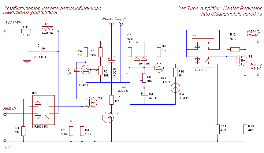
2. Filament key-stabilizer and timers
Zest key-stabilizer - in two pass transistors, in the two most typical the ignition modes (11.5-12.0 In the Parking lot, 14.0-14.5 In in motion) work with minimal heat generation. In the movement is open T2, T1 is closed, the over voltage falls to R5. The resistance R5+Rcи(T2) is equal to 3V/Nagruzke. Parked both transistor is opened, the current flows through T1, which scatters P=Nagruzki*Rcи (of the order of tens milliwatts). T1 must have standard, not "logical" the levels are Easy. Rси T2 uncritical, T1 is not more than 100 mω (at the rate of losses 300mV at 3A load current). If the task thermal discharge T1, T2 is not (there is a decent radiator, put T2 with Rcи=1 Ohms (for current 3A) and totally remove R5. I put IRFI540, without a radiator (cooling T1 provided by a large the square of the flow paths and the source.
Anodic timer uses in as a pass element optocoupler, timer relay - P-TIR transistor, or p-n-p transistor (CT, you will need to reduce the resistors R12-R13) controlled by optocouplers. When removing the REM signal IN all capacities, located after the key TT, quickly discharged on the filament lamps, ensuring the establishment of the timer in the status "off" even when short-term deposition IN REM.
3. Anodic stabilizer
To simplify the topology used with the push-pull circuit one N-TIR key on the shoulder. These transistors must have not Rси above 15, 20 mW in order to avoid excessive losses. Again for the purpose to simplify the topology used IP EU (UC3825) - does not require external drivers shutter. IP included with OS voltage optocoupler interchange, clock frequency KC. Overcurrent protection at 12V input the power is not needed - transistors able to withstand briefly overloaded, then I fuse. Protection the fall of the supply voltage when neobhodimosti is easy the inclusion of 1.5 V of the Zener diode in the circuit the power of IP.
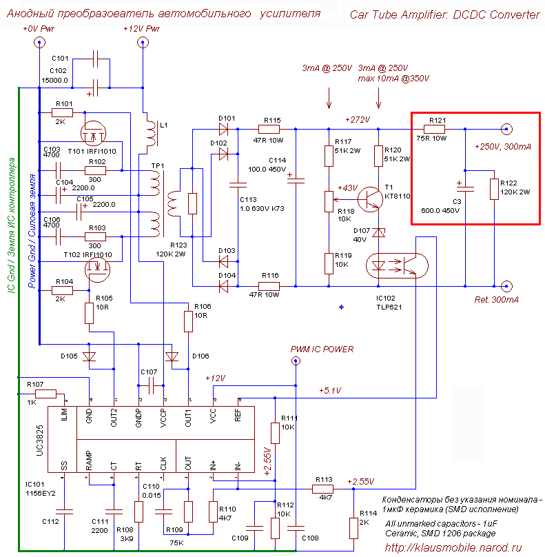
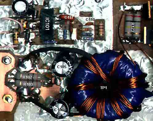
Transformer at the ring M1500 38*24*14, machined to elliptic section. First performed the secondary winding (140 turns = 2 layer the Litz wire brand unknown to me, about 0.2 sq mm total section), then primary (2*4.5 turns, 7 KOs lived sew 0.75 mm). The rectifier bridge The Greek, to do one the secondary winding.
Snobbery installed and in primary and in the secondary circuit. In the secondary circuit is the role of the snubber performs just a resistor on the input diode bridge, without tanks (they then would need is very small). CRCRC filter (СRCR on-Board MON, last, red frame - the Board ULF). First in the chain - K73-17 630V, further electrolytes. Choke I 't put as resistor and enough, and the extra amplitude recess on the throttle here to anything. Chain OS removes the output level with the second filter capacitor. When this loop turns completely sustainable (load 0-300mA, the output voltage 150-300V).
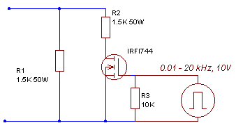
The sensor circuit intentionally OS made a relatively low-impedance - it provides the load filter at no-load and discharge containers when turned off. In point stabilization (led current optocoupler 1.5 .. 3 mA) current consumption bit increases with chain approximately 4 to 8 mA - a kind of stabilizing shunt working in parallel with the loop OS PWM. For sustainability OS coefficient the gain of the error amplifier relatively small (approximately 15). To test the effectiveness stabilization using a simple resistive load:
Attention! Depending on execution, R105-106 can be reduced to 2-5 Ohms or eliminate altogether.
4. Implementation
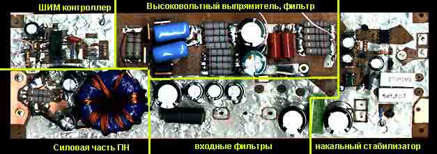
Fee bilateral, 260*80mm (in fact, the components occupy 250*60mm). The anode circuit divorced only on the upper side of the Board without vias (surface mount). T1, T, T, located under the card (refer the bottom chassis, which is the radiator. The total heat sink no more than 7-10W).
Drains T, T onto the upper side of the Board to contact site about 8*15mm, which top soldered the findings of the primary and R102, 103. The origins T, 102 and negative nogo S, 106 onto the top layer of the earth. S, 106 shunted the chip 1uf capacitors (SMD 1206), soldered between pins S, 106 directly at their base. Similarly, the locking capacitors of findings 8,11,15,16 IC101 unsoldered from the lower and upper sides Board. S should be enough thermostable.
Here, perhaps, and all. Success!
Publication: www.klausmobile.narod.ru, www.cxem.net