


")

Attention radio Amateurs will be designing the power supply for home lab. The advantage of this PSU that don't need an additional winding on the power transformer. DA1 chip single-supply operation. The output voltage is continuously adjustable from 0 to 30 V. The PSU has a smooth adjustment of the current limit.
Circuit solution is easy and this power unit can produce a radio Amateur.
The rectified voltage is +38, after the capacitor C1 is supplied to the control transistor and the transistor VT2 VT1. Transistor VT1, diode VD2, the capacitor C2 and the resistors R1, R2, R3 assembled stabilizer, which is used to power the chip DA1. Diode VD2 is a three-terminal, adjustable parallel to the voltage regulator. [2] At the output of the regulator, resistor R2 sets the voltage and +6.5 volts, because the marginal supply voltage circuits DA1 VDD = 8 volts. At the operational amplifier DA1.1 TLC2272 [ 1 ] collected governing part of the power supply voltage. Resistor R14 is regulated by the output voltage of the power supply. On one of the contacts of the resistor R14 is supplied reference voltage is 2.5 volts. The accuracy of this voltage within a narrow range is set by the selection of resistor R9.
Through the resistor R15, the adjustable resistor R14, a voltage is applied to the input 3 of the operational amplifier DA1.1. Through this operational amplifier processing the output voltage of the power supply. Resistor R11 is regulated by the upper limit of the output voltage. As already mentioned, DA1 chip fed by a single power 6,5 V. And yet, at the output of the PSU managed to get the output voltage is equal to 0 V.
On the chip DA1.2 built knot protect the flanks of the power-current and short circuit. Such circuit design node protection has been described in many different RL literature and therefore not described in detail.
In the author's version current can be adjusted from 0 to 3A. Chain R10 and VD4 is used as an indicator of over-current and short circuit.
Schematic diagram of the power supply unit shown in Fig. 1.
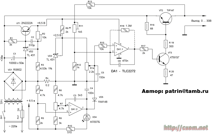
Fig. 1
The establishment of the PSU start with a supply voltage of +37…38 V. the capacitor C1. Resistor R2 exhibit a collector voltage VT1 +6,5 V. Chip DA1 in the socket is not inserted. After the output voltage at the 8 foot panels DA1 set +6.5 V, turn off the power and insert into the socket chip. After turn on the power and, if the stress on the leg 8 DA1 differs from +6.5 V, make the adjustment. Resistor R14 you should see 0, i.e. in the bottom in the diagram position.
After the supply voltage of the chip is installed, set the reference voltage of +2.5 V on the upper output of the variable resistor R14. If it differs from that specified in the scheme, choose a resistor R9. Thereafter, the resistor R14 is transferred to the upper position and a trimming resistor R11 sets the upper limit of the output voltage +30V. The output of the lower voltage without the resistor R16 is equal to 3.3 mV that does not affect the reading digital display and indications equal to 0V. If between the legs 1 and 2 circuits DA1.1, insert a resistor of 1.3 MW., the lower limit of the output voltage decreases to 0.3 mV. Pads of the resistor R16 is provided in the circuit Board. Then connect the rheostat resistance in the load and check the site settings of protection. If necessary, choose the resistors R6 and R8.
In this design you can use the following components.
VD2, VD3 - KPU2EH19, instead of TIP147 transistor VT2 you can use native transistor CT, VT3 - BD139, BD140, VT1 - any flint low or medium power transistor with a voltage IR at least 50V. Trimmer resistors R2 and R11 from the SP5. The power transformer can be applied at a power of 100 … 160W. Resistor R16 to the characteristic TC better than 30 ppm/ Co and must be either a wire or metal-foil type. The power supply is built on a printed circuit Board size 85 x 65 mm.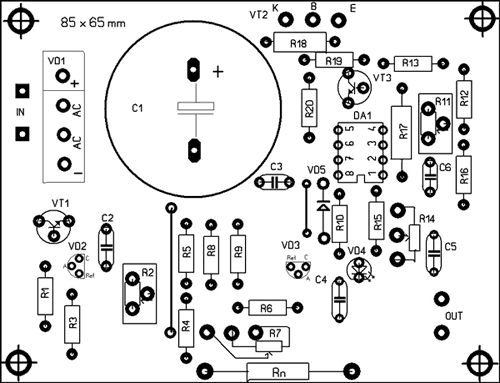
Fig. 2
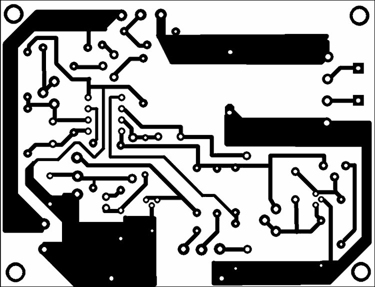
Fig. 3
The node of the reference voltage VD3 can be replaced by a node on the chip TLE2425 - 2,5 [3] the Input voltage of the chip may vary from 4 to 40 V. the Output voltage is stable - 2.5 V.
During tuning chips instead of TLC2272 was applied experimentally chip TLC2262. All parameters remained equal to the specified deviations modes were observed.
During testing of this design on the power of the chip was not filed 6.5 V, and 5 V. In this case, the resistor R9 = 1,6 K. Node power the chip was replaced with a unit as shown in Fig. 5.
If the chip TLC2272 not in DIP-8 and SOIC-8, then we can proceed as follows, without rewriting the PCB. From the isolated material is prepared, the substrate is a rectangle measuring 20 x 5 mm On this rectangle, glue "The MOMENT", attached the legs to the top", i.e. upside down, chip. The location of the chip on the substrate shown in Fig. 6.
Then, the resulting "sandwich" paste, all with the same glue on the reverse side of the PCB after removing the socket DIP-8 (if it was waives). The substrate with the chip is glued, with evenly between the contact pads of the chip on the circuit Board. Leg 1 of the chip should be opposite the pads belonging to the leg 1 circuits DA1, or moved a little lower. After this operation, the flexible wires and soldering connecting the legs of the chip and contact pads on the circuit Board.
The hams were collected several copies of the data blocks of nutrition. They all started to work immediately and showed the specified results.
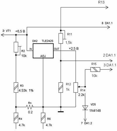
Fig. 4
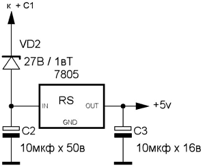
Fig. 5
Also, the design took into account not expensive base parts, a minimum of parts, ease of establishment and circulation, as well as output parameters, the most acceptable among radio Amateurs.
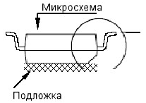
Fig. 6
Literature
[1] http://radiodetail.narod.ru/m_i/m_i_tl/tlc2272.htm
[2] http://www.promelec.ru/pdf/tl431_on.pdf
[3] http://www.itc-electronics.com/CD/Texas_10166_Analog-Mixed-2003/docs/html/datasheets/slos065d.pdf
Publication: www.cxem.net