


")

Now the house has a lot of small equipment that requires constant power. This watch with led indication, and thermometers, and small receivers, etc., In principle, they are designed for the batteries, but those "sit down" at the most inopportune moment. Easiest way is to feed them from the network power supply units. But even a small-size network (step-down) transformer quite heavy and is not so little, and pulse power sources still complicated and require for making certain experience and expensive equipment.
The solution to this problems under certain conditions can serve as a transformerless the power supply capacitor with damping. These conditions are:
- full autonomy as a powered device, i.e. it should not connect any external devices (such as a receiver for a tape recorder recording program);
- dielectric (non-conductive) housing and handle control the power supply unit and connected to the device.
This is due to the fact that when powered by a transformerless block device is under the capacity of the network, and the touch on his bare elements can "shake". It is useful to add that when setting up these power supplies must comply with the rules safety and caution.
If necessary use for setting up the oscilloscope power supply must be switched via an isolation transformer.
In its simplest form diagram of a transformerless power supply is shown in Fig.1.
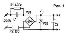
To limit inrush current when connecting the unit to the mains in series with the capacitor C1 and rectifier bridge VD1 included resistor R2,and to discharge the capacitor after the off - parallel to the resistor R1.
Transformerless power source in the General case is a symbiosis rectifier and parametric stabilizer. The variable capacitor C1 current is a capacitive (reactive, i.e. it does not require energy) the resistance of HDL, the value of which is determined by the formula:
where (- mains frequency (50 Hz);-capacity of the capacitor C1, F.
Then the output current of the source can be approximated as:

where Uc is the voltage (220V).
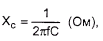
The input portion of the other of the power unit (Fig.2A) contains a ballast capacitor C1 and bridge rectifier from diodes VD1, VD2 and Zener diodes VD3, VD4. Resistors R1, R2 play the same role as in the first the schema. Waveform of output voltage of the power is shown in Fig.2B (when the output voltage exceeds the voltage stabilizing Zener, otherwise it works like a normal diode).
From the beginning the positive half cycle of the current through the capacitor C1 to the moment t1 the Zener diode and diode VD3,VD2 opened, and a Zener diode VD4 and diode VD1 closed. In the time interval t1…t3 Zener diode VD3 and diode VD2 remain open, and through the opened Zener diode VD4 passes the current pulse stabilization. The output voltage and Uвых the Zener diode VD4 equal its voltage stabilization East.
The pulse current stabilization, which is diode-rectifier stabilitron pass-through, pass the RH load, which is connected to the output of the bridge. At the time t2 the current stabilization reaches a maximum, and at the time t3 is equal to zero. Before the end of the positive half cycle remain open Zener diode VD3 and diode VD2.
At the time t4 and ends with positive begins with negative half-cycle, from start until t5 already Zener diode VD4 and VD1 are open, and a Zener diode and a diode VD3 VD2 closed. In the time interval t5-t7 Zener diode VD4 and diode VD1 to remain open, and through the Zener diode VD3 at the voltage UCT passes through the current pulse stabilization, the maximum in the time t6. From t7 to the completion of the negative half cycle remain open the Zener diode VD4 and the diode VD1. Reviewed the cycle of operation of the diode-stabilitron rectifier is repeated during the following periods mains voltage.
Thus, through the Zener diodes VD3, VD4 from the anode to the cathode passes rectified current, and in the opposite direction pulse current stabilization. In the time intervals t1…t3 and t5 t7…voltage stabilization does not change more than a few percent. The value of the variable power input bridge VD1 VD4 in… the first approximation is equal to the ratio of voltage to a capacitive resistance the ballast capacitor C1.
The operation of the diode-stabilitron rectifier without ballast capacitor, bounding the through current is not possible. In functional they are inseparable and form a single whole - condenser-stabilitron the rectifier.
The variation UCT-type Zener diodes is approximately 10%, which leads to additional output voltage ripple with the mains frequency, the amplitude of the voltage ripple is proportional to the difference values East of Zener diodes VD3 and VD4.
When using powerful Zener DA…DG they can be mounted on a common heatsink, if the designation of their type are the letters "PP (Zener DAP…have DGP reverse the polarity of the findings). Otherwise, the diodes and Zener diodes must to swap.
Transformerless power sources are normally collected by the classical scheme: the quenching capacitor, rectifier AC voltage, a filter capacitor, the stabilizer. Capacitive filter smoothes the output voltage ripple. Than more capacitance of the filter, the less ripple and, therefore, more constant component of the output voltage. However, in some cases, can without the filter, which is often the most cumbersome a node of such a power source.
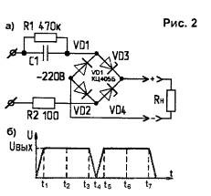
It is known that a capacitor in the circuit of the alternating current, shifts its phase 90°. Phase-shifting capacitor is used, for example, when connecting three-phase motor to a single phase. If the rectifier to apply phase-shifting capacitor, providing mutual overlap of half the rectified voltage, in many cases you can do without bulky capacitive filter or significantly reduce its capacity. Scheme such stabilized rectifier shown in Fig.3.
Three-phase rectifier VD1.VD6 connected to a source of AC voltage active (resistor R1) and capacitance (capacitor C1) resistance.
The output voltage of the rectifier stabilizes the Zener diode VD7. Phase-shifting capacitor C1 must be rated in AC circuits. Here for example, suitable type capacitors K73-17 with an operating voltage of not lower than 400 V.
This rectifier can apply where it is necessary to reduce the size of electronic devices, because the size of capacitors capacitor filter as a rule, much more than a phase-shifting condenser of relatively small capacity.
Another advantage the proposed option is that current consumption is almost constant (in the case of constant load), whereas in rectifiers with capacitive filter in the moment of switching inrush current significantly exceeds the established value (due to the charge in the capacitors of the filter), which in some cases is extremely it is undesirable.
The described device can be applied with consistent voltage regulators with constant load and with load, does not require voltage regulation.
Completely unpretentious transformerless power supply (Fig.4) can be built "on the knee" literally for half an hour.
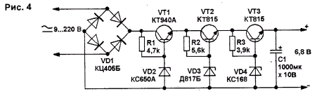
In this embodiment, the circuit designed for the output voltage of 6.8 V and a current of 300 mA. The voltage can be changed the replacement of the Zener diode VD4 and, if necessary, VD3 And setting the transistors the radiators can be increased and the load current. Diode bridge - any designed for reverse voltage not less than 400 V. Incidentally, can to recollect about "ancient" diodes. DB.
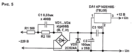
In another transformerless source (Fig.5) as the stabilizer used chip KREN. Its output the voltage is 12 V. If the output voltage regulation, pin 2 IC DA1 connect to GND through a variable resistor, for example, type SPO-1 (linear characteristic changes in the resistance). Then the output voltage can must be in the range 12…22 V.
As a chip for DA1 other output voltages need to apply appropriate integrated stabilizers, for example, KREN, KREN,CREA Capacitor, etc. C1 must be on the operating voltage of not lower than 300 V, the brand K-3, K73-17 or similar (non-polar, high voltage). The oxide capacitor C2 acts as a filter on nutrition and smooths out the ripple voltage. Capacitor C3 reduce noise at high frequency. Resistors R1, R2 - type MLT-0,25. Diodes VD1…VD4 can be replaced by KD105B…CDG, CDA, B, CDE. The Zener diode VD5 with voltage stabilization 22…27 protects the chip from surges at the moment of inclusion of the source.
Although theoretically capacitors in an AC circuit power do not consume, in reality they are due to the presence of losses can be allocated some the amount of heat. To check the suitability of the capacitor as the quenching for use the transformerless UPS can simply plugging outlet and estimating the temperature of the hull in half an hour. If the capacitor time to warm up noticeably, it is not appropriate. Virtually no heat special capacitors for industrial installations (they are designed for large reactive power). These capacitors usually are used in fluorescent lamps, electronic control devices induction motors, etc.
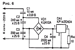
A 5-V source (Fig.6) with load current up to 0.3 A applied the capacitor voltage divider. It consists of a paper capacitor C1 and two oxide C2 and C3, forming a bottom (under the scheme) nonpolar shoulder capacitance 100 UF (anti-series connection of capacitors). Polarizing diodes for oxide pairs serve the diodes of the bridge. Under these component values of the short-circuit current at the output of the power supply unit is $ 600 mA, the voltage across the capacitor C4 in the absence of load - 27 V.
Unit for powering portable receiver (Fig.7) fits in it the battery compartment. Diode bridge VD1рассчитывается on the operating current, its marginal the voltage determined by the voltage that provides the Zener diode VD2. Elements R3, VD2. VT1 form a powerful analogue of the Zener diode. The maximum current and power dissipation of this Zener diode is determined by the transistor VT1. For you may have a radiator. But in any case, the maximum current that the transistor must not be less than the load current. Elements R4, VD3 - chain the indication of the output voltage. At small load currents must take into account the current consumption of this circuit. Resistor R5 load the power circuit is a small current than it stabilizes.
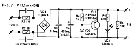
The quenching capacitors C1 and C2 - type KBG or similar. Can also apply K73-17 with an operating voltage of 400 V (with 250 V, as they are connected in series). The output voltage depends on the resistance the quenching capacitor to alternating current, actual load current and voltage the Zener voltage.
To stabilize voltage transformerless power supply with damping capacitor can use a symmetrical discs (Fig.8).
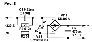
When charging the filter capacitor C2 to a voltage opening dynistor it turns on and VS1 bypasses the input diode bridge. The load at this time receive power from the capacitor C2 At the beginning of the next half cycle C2 again charged to the same voltage, and the process repeats. Initial voltage discharge of the capacitor C2 does not depend on the load current and voltage, so the stability of the output voltage of the unit is high enough.
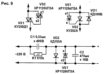
The voltage drop on the diacs in the on state is small, power dissipation, and hence, and heat it considerably less than that of the Zener diode. The maximum current through a dinistor is about 60 mA. If to obtain the necessary output current this value is not enough, you can "umonit a dinistor a triac or thyristor (Fig.9). The lack of such sources of power - limited output voltage determined by the voltage inclusion of diacs.
Transformerless the power supply with adjustable output voltage is shown in Fig.10A.
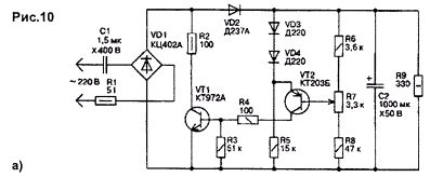
Its peculiarity lies in the use of adjustable negative feedback connection from the output of the unit at cascade transistor VT1 connected in parallel to the output the diode bridge. This cascade is the regulatory element and is controlled by a signal output from a single stage amplifier to VT2.
The output signal VT2 depends on the difference of voltage supplied from the AC resistor R7 connected in parallel to the output of the power supply, and reference the voltage on the diodes VD3, VD4. Essentially, the scheme represents a adjustable parallel stabilizer. Role the ballast resistor plays a quenching capacitor C1 parallel to the managed element, the transistor VT1.
Runs this block power as follows.
When included in a network transistors VT1 and VT2 are locked and through the diode VD2 is happening the charge storage capacitor C2. When reached on the basis transistor VT2 voltage equal to the reference diodes VD3, VD4, transistors VT2 and VT1отпираются. The shunt transistor VT1 the output of the diode bridge, and its output voltage drops, which leads to reducing the voltage on the storage capacitor C2 and to the locking transistors VT2 and VT1. This, in turn, increases the voltage on C2, unlocking VT2, VT1 and the repetition of the cycle.
Due to the current thus negative feedback output the voltage remains constant (stable) as with the load switched on (R9) and without it (at idle). Its value depends on the position of the engine potentiometer R7.
Top (the scheme), the position of the slider corresponds to a larger output voltage. Maximum the power output of those devices is equal to 2 watts. The limits of adjustment the output voltage from 16 to 26 In, and when shorted диодеVD4 from 15 to 19.5 V. the ripple at the load is less than 70 mV.
Transistor VT1 works in alternating mode: when there is load in the linear mode, the idling - mode pulse width modulation (PWM) with a frequency of the ripple voltage on the capacitor C2 100 Hz. In this case, the voltage pulses at the collector VT1 have flat fronts.
The criterion of correctness selection of capacitor C1 is to obtain the desired maximum load voltage. If its capacity is reduced, the maximum output voltage on rated load is not achieved. Another selection criterion C1 is the constancy of the voltage waveform at the output of the diode bridge (Fig.10B).
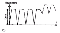
The voltage waveform has the form of a series of rectified sinusoidal half waves of the mains voltage with limited (flattened) the positive peaks of palusinski, the amplitude of the peaks is variable quantity that depends on the position of the engine R7, and varies linearly with its the spin. But each wave must necessarily reach zero, the presence of a constant component (as shown in Fig.10B the dotted line) is not allowed because it violates the stabilization mode.
Linear mode is a lightweight, transistor VT1 is heated a little and maybe to work almost without a radiator. Small heating occurs in the lower the position of the slider R7 (minimum output voltage). At idle the thermal regime of the transistor VT1 is deteriorating in the upper position of the engine In R7 this case, the transistor VT1 needs to be mounted on a small heatsink, for example, in the form of a "box" of aluminum plate square of side 30 mm and a thickness of 1…2 mm.
The control transistor VT1 - average power, with a large coefficient transmission. Its collector current must be 2…3 times greater than the maximum load current, the allowable voltage the collector-emitter is not less than the maximum output voltage of the power supply. In as can VT1 to be used transistors CTA, CTA, CTA etc Transistor VT2работает in the regime of small currents, so we're all on the low-power p-n-p transistor - CT, KT361, etc.
Resistors R1, R2 - protective. They protect the control transistor VT1 from failure due to overcurrent transients at the moment switching the unit to the network.
Transformerless condenser rectifier (Fig.11) works with autostabilization output voltage. This is achieved by changing the time connect the diode bridge for the storage capacitor. In parallel to the output diode bridge the transistor VT1, operating in key mode. Base VT1 through the Zener diode VD3 connected with a storage capacitor C2, separated DC output from the bridge diode VD2 to exclude rapid discharge when open VT1. While the voltage on C2 is less than the voltage stabilization VD3, the rectifier operates as usually. If you increase the voltage on C2 and opening VD3 transistor VT1 also opens and bypasses the output of the rectifier bridge. The output voltage of the bridge abruptly decreases almost to zero, which leads to a decrease the voltage on C2 and off of the Zener diode and switching transistor.
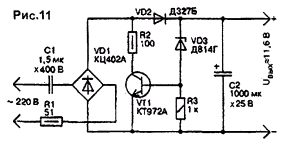
Further, the voltage on the capacitor C2 increases again before the inclusion the Zener diode and transistor and so on led output voltage very similar to the operation of a pulse voltage with a pulse width regulation. Only the proposed device frequency pulse is equal to the frequency of the ripple voltage on C2. Key transistor VT1 for reduce losses should be with high gain, for example, CTA, CTA, CTA and others to Increase the output voltage of the rectifier by applying more high-voltage Zener diode (chain low-voltage, United consistently). When two Zener DV, DD and the capacitance of the capacitor C1 2 μf output voltage across the load resistance 250 Ohm can be 23 24 V....
It is similarly possible to stabilize the output voltage half-wave diode-capacitor rectifier (Fig.12).
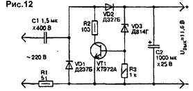
To rectifier positive output voltage in parallel with the diode VD1 included n-p-n transistor, driven from the output of the rectifier through the Zener diode VD3. When the capacitor C2 voltage corresponding to the time of opening Zener diode, the transistor VT1 is also open. As a result, the amplitude of the positive half of the voltage arriving at C2 through the diode VD2, is reduced almost to zero. When reducing the voltage on C2 transistor VT1 due to the Zener diode is closed, which leads to an increase the output voltage. The process is accompanied by a pulse-width control pulse duration at the entrance VD2, therefore, the voltage on the capacitor C2 is stable.
In the rectifier negative output voltage in parallel with the diode VD1 need to include p-n-p transistor CTA or CTA. Stabilized output voltage at the load the resistance of 470 Ohms to about 11, the voltage ripple of 0.3…0.4 V.
In both embodiments, the Zener diode operates in a pulsed mode at a current in units milliamps, which is not connected with the load current of the rectifier, scatter the capacity of the quenching capacitor and voltage variations. Therefore, the loss in it significantly reduced, and the heat sink is not required. Key transistor radiator also it is not required.
Resistors R1, R2 in these schemes limit the input current transients at the moment of switching devices in the network. Because of the inevitable bounce contacts plug the process of inclusion is accompanied by a series of short-circuits and breaks the circuit. When one of these circuits quenching capacitor C1 can be charged to full the peak value of the mains voltage, i.e. approximately up to 300 V. After the break and subsequent circuit because of the "bounce" that the mains voltage can to take shape and form in the amount of about 600 V. This is the worst case, which you must consider to ensure reliable operation of the device.
Another option key transformerless circuits the power source is presented in Fig.13.
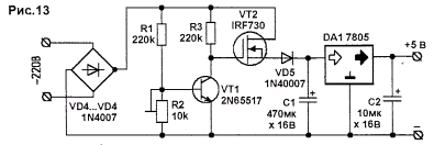
Mains voltage, passing through the diode bridge наVD1.VD4, converted in pulse amplitude of about 300 V. the Transistor VT1 comparator, VT2 is the key. Resistors R1, R2 form a voltage divider for VT1. Adjusting R2 set the voltage comparator. While the output voltage diode bridge reaches a certain threshold, the transistor VT1 is closed, gate VT2 - gate trigger voltage, and it is open. Through VТ2 and the charging diode VD5 the capacitor C1.
When reaching the set threshold transistor VT1 is opened and bypasses the valve VT2. The switch closes and opens again when the output voltage of the bridge will be less than the threshold of the comparator. Thus, C1 is set the voltage that stabilizes the integral stabilizer DA1.
Shown in the diagram the values of the power supply provides an output voltage 5 V at currents up to 100 mA. Configuration consists of setting the threshold VT1. Instead IRF730 can use. CPA, IRF720, BUZ60, 2N6517заменяется on CTA.
Miniature transformerless power supply for low power devices can be build on the chip HV-2405E (Fig.14), which performs direct conversion of AC voltage to DC.
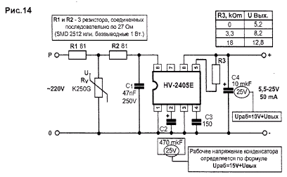
Range input voltage IC -15…275 V. the output - 5…24 V with a maximum output a current of 50 mA. Available in flat plastic package DIP-8. Structure the chip is shown in Fig.15A, the Pinout is shown in figure.15B.
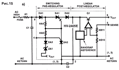
In the schema of the source (Fig. 14) special attention should be paid to the resistors R1 and R2. Their the total resistance should be in the region of 150 Ohms, and the power dissipation is not less than 3 watts. Input high voltage capacitor C1 may have a capacitance of from 0,033 to 0.1 UF. Varistor Rv possible apply with virtually any operating voltage V. 230.250 Resistor R3выбирается depending on the required output voltage. In its absence (outputs 5 and 6 are closed), the output voltage of slightly more than 5 V, the resistance of 20 ohms the output voltage is about 23 V. Instead of the resistor can include a Zener diode with the necessary voltage stabilization (5 to 21). For other parts there are no special requirements, except for the choice of working voltage electrolytic capacitors (formula for calculation, see the scheme).
Given the potential the danger transformerless sources, in some cases, may represent the interest of compromise: with damping capacitor and transformer (Fig.16).
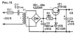
Here goes the high-voltage transformer with a secondary winding, as necessary the rectified voltage is set by selecting the capacitance of the capacitor C1. Importantly, winding of the transformer to provide the required current.
The device will not out of order when disconnecting the load to the output of the bridge VD1…VD4 should connect the Zener DP. In normal mode it does not work because it the voltage stabilization above the operating output of the bridge. Fuse FU1 protects transformer and stabilizer in the breakdown of the capacitor C1.
The sources of such type in the chain sequentially United capacitor (the capacitor C1) and inductive (transformer T1) resistance may be a resonance voltage. Keep this in mind when their establishment and control voltage with an oscilloscope.
Author: V. Novikov