


")

We have repeatedly been told about the methods of improving the reliability phones automatic determination of the number of the caller (caller ID), powered from the network AC. Some of the devices restart could not work with all software versions. There were other limitations. The proposed article options devices of protection against failures that can to use the phones on the Z80 processor, and in the other caller ID.
Consider the main causes unstable operation of caller ID.
1. Failures due to impulse noise in the mains. Strong domestic disturbances create devices containing power transformers or motors, especially a refrigerator. In my experience, the best protection is to select a power Aona separate a socket connected to the wiring as far as possible from such devices.
2. The build quality of the device. Let me emphasize that the test I conducted only on the caller ID collected on high quality printed circuit boards, having a good pike (aka is it worth spending the time and effort to upgrade?). The panels, in which chip installed, should ensure a reliable contact. When the slightest suspicion of the poor quality of their sockets must be replaced.
3. Transients if power is the cause of the vast most failures. The most typical consequences of this for the caller ID on the Z80 these are:
- the appearance of extraneous digits and characters in the files of incoming and outgoing calls, the notebook buffer;
- indiscriminate filling of alarm information;
- change the operation mode of the phone and user constants that can seriously make it difficult to work with the device;
- the failure of the current time and date;
- the wrong response to the call;
- spontaneous "hang", in which the possible occupation of the telephone line without the user's knowledge.
Failures of the last two categories and the like have very sad consequences, as associated with distortion not available to the user of system variables program Aona. This leads to "hang" of the processor and subsequent restart with complete loss of stored information in the RAM. Often, such a failure does not causes freezing, but remains in memory and later manifests itself like a computer virus, creating the illusion of operability of the apparatus. For this because of the protection device that monitors the scan indicator, not always effective. Does not solve the problem and disabling tire processor signal BUSRQ (for Z80).
Unfortunately, these shortcomings inherent in the caller ID made on another element base, in particular on micro-computers s. Better protected against failures devices that use FLASH memory.
Analysis of Aona shows that the cause of these phenomena is inadequate study of the digital part of the device. In particular, when the voltage power from +5 V to zero (disabling electrical energy ) signals WR and RD for the inputs of chip RAM some time are of uncertain value, since the voltage on these lines falls synchronously with the feeding. Prohibiting same level such signals for RAM - high. In addition, there is the probability of false select RAM signal CS. The combination of these two factors can lead to spurious actuation of the RAM, the entry in which the information for it is not designed, creates the above-described effects. False select RAM mode reading is also harmful: when the tire data starts to be fed from the condenser support RAM. In total for 2…3 it is discharged by more than half. Naturally, long-term storage of data in RAM.
The most effective way to protect against such failures includes control the voltage block RAM when the voltage drops below the a certain level. When the inhibit signal generated at the CS input chip RAM, disables it on all the time of the transition process. Thanks excluded as distortion of information in memory, and rapid discharge of the capacitor support.
The proposed method has a very high efficiency (more than 99%) as eliminated not only the consequences but also the cause of failures. Such protection applies in devices with any version of firmware, with different types of processors (as Z80 and a single-chip micro-computers) and RAM (both two-and vosmigigabaytnyie), i.e. almost all the caller ID using the power from outlet. The downside is the lack of protection from surges. If this a problem does arise, you can optionally use the device restart for the Z80, for example, as indicated in [1]. In the caller ID based on micro-computers the device is automatically restarted, it is usually part of the apparatus.
In Fig. 1 shows a basic version of the protection device and connecting it to the model the scheme Aona on the Z80 using RAM 2 Kbytes. Designation of items on Board Aona matches [2]. The comparator DA1 used as a trigger Schmitt, levels of response depend on the ratios of the resistors R3 - R5 (practically important only the value of the lower threshold).
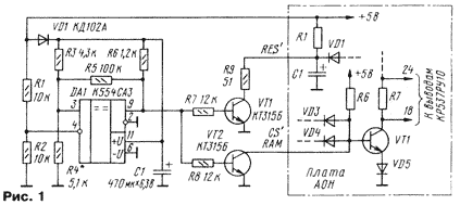
When the supply voltage drop (and hence the voltage at pin 4 DA1) to some value, at pin 9 DA1 there is a high level. Transistors VT1 and VT2 open, and the transistor that controls the sample RAM Aona is closed. The capacitor in the circuit of the CPU reset is quickly discharged through outdoor transistor VT1, which protects the processor from "hang" for short (less than 2) power outage. The power of the comparator during the transition process provides a capacitor C1.
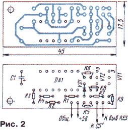
In the device used resistors MLT, capacitor C1 - C50-35. Drawing the PCB shown in Fig. 2.
For establishing devices need a digital voltmeter with an input resistance not less than 1 MW and a resolution of better than 0.01 V. First resistor R4 should be replaced a chain of series-connected constant resistor of 2 ohms AC and 4.7 Ohm, and the engine last set minimum resistance. Then measure the voltage at pin 4 of the chip DA1 and, slowly rotating the engine, variable resistor, set at pin 3 DA1 the voltage at 0,04 0,08…In lower measured.
Note that a potential difference of more than 0.1 In can lower the effectiveness of the protection, if too small the difference may appear false actuation, for example, due to thermal instability elements. When measurement is necessary to ensure that the comparator could not be switched into a state a high level on pin 9.
After that, measure the circuit resistance of the two resistors and replace it with one constant resistor, which is matched as accurately as possible. Customized fee place in the case of caller ID, while the connecting wires should be done as short as possible.
To test the protective properties you want to enable caller ID to the network and restart the program (in particular, for versions of "Rus" press: "&№42;", "&№42;", "3", "5", "1"). Then repeatedly (30-40 times) to lead a series of off-vklyucheniyami using electroclinical with built-in switch. After this it is necessary to view the contents of the memory areas Aona, available to the user: archives incoming and outgoing calls, notebooks, alarm clocks. The lack of information in them indicates the reliability of protection. It is also useful to view user constants, comparing them with the values located in memory after a restart. If failures in memory yet discovered, the setting should be repeated (see above) by setting the resistor R4 a bit more resistance.
Now a few words about the capacitor recharge RAM in One. Most to consider the capacity of 220…470 µf. The main role is played not by the value of the capacitance, and the quality of the insulation, i.e. the leakage current. The type of capacitor selected experimentally. So, cheap Chinese made capacitors and domestic C50-35 is able, as a rule, to maintain nutrition RAM for 3…4 hours For capacitors with a lower leakage current of the storage time can be calculated for days and even exceed one week (the author makes use of capacitors firms NITSUKO). The best option is the use of ioniser or batteries of 2-3 the "fingerprint" of elements that are connected through the diode, it makes the phone memory practically nonvolatile. For placement of elements it is convenient to use the battery cover, available in many models, in particular "Technica".
Another comment relates to the supply unit (PSU) Aona: the sensitivity of the protection device places high demands on him. The presence of visible pulsations is highly undesirable, and in some cases actually unacceptable (especially if you have installed a very small potential difference between the inputs of the comparator, see above). Therefore, you should test the PSU under load: the minimum instantaneous voltage at the input of the stabilizer CREA not should be below 8.5 V, it is Useful to test the source and at low voltage in network, using Latr. In the case of the output ripple should to replace the PSU or to take measures for their improvement: to increase the number of turns of the secondary winding, replace the rectifier with an average point on the pavement, all powered by winding, etc.
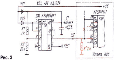
The second variant of the protection device shown in Fig.3. The basis of it is integral timer DA1 included atypical: UR input (pin 5) is used for supply of operating and R (pin 6) is a reference voltage. The Divider R1 R2 allows you to set between pins 5 and 6 DA1 voltage of several hundredths volt, which determines the sensitivity of the device.
The principle of operation is the same as in the first embodiment: in the event of power the voltage at pin 5 DA1 decreases much faster than that at pin 6, in the end triggered comparator upper level, a part timer DA1 and output DA1 occurs low. On subsequent power-on the chip outputs DA1 is held high level due to the action of the comparator low level input (pin 2 DA1) is connected to GND [3].
The DA1 output with push-pull output stage (pin 3), is used to lock the RAM of the device. Depending on applied in One CPU and RAM possible one of the three options you enable.
1. In the apparatus used RAM CRRU or similar, regardless of processor type. In this case, we use the non-inverting input CS (pin 26) chip RAM, which is usually not involved and connected to the positive output the power source. Should the specified output is disconnected from the power supply circuit and submit to him a signal directly from the output 3 chip DA1. Resistor R&No. 39;, support input CS inactive level in the storage mode, it is necessary to mount on-Board Aona (Fig.3).
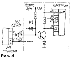
2. Used RAM CRRU (RU), a sampling scheme which contains the transistor [4]. Such a construction of a node is used in almost all vehicles on the Z80 and pretty rarely in other caller ID. In this case it is necessary to use a diode VD3 and connect conductor with its anode to the base of the aforementioned transistor, as shown in Fig.4.
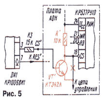
3. Used RAM CRRU (RU), a sampling scheme which has not of the transistor. This connection is typical of most of caller ID on the basis of micro-computers (for example, C) and is extremely rare in the apparatus on the Z80. The lock is on the CS input (pin 18) chip RAM, on cost Aona set the transistor VT and resistor R&No. 39; (Fig.5). Need cut in a convenient location printed wire that goes to the specified output chips, and neatly soldered to him the conclusions of the transistor emitter and the manifold. To the withdrawal of the base VT&No. 39; connect a conductor from protective devices, when instead of the diode VD3 install the resistor R3. Resistor R&No. 39; is installed on Board Aona between pins 18 and 24 of chip RAM.
It should be noted that all of the different types of foreign chip RAM, used in the caller ID, in practice, limited to two types of chips, different capacity: 2 Kbytes and 8 Kbytes. In particular, the chip having 24 o, are analogues of domestic appliances CRRU (RU) as functional purpose and location of the findings. Similarly, foreign chip, implemented in 28-pin packages, interchangeable with the domestic CRRU. Separately, you can mention chip FLASH memory (usually manufactured in 8-pin packages); they are used in relatively caller ID rarely and do not require any protection from interference due to other physical the principle of operation.
The timer output DA1 open collector (pin 7) is used to restart of the processor. In the case of the Z80 enough to find on the Board Aona capacitor circuit initial run, to the positive output of which is connected with the conductor the specified output DA1.
In the caller ID made on a single-chip micro-computer, the security device complements factory system to automatically restart, making it work more correctly. To implement the protection you first need to find the wire that goes to the reset input microcomputer (for example, s DIP in this conclusion 9 [4]). Then identify logical elements involved in the operation of the system is restarted (usually it runs on chips K561LN2 or CLE), and, finally, a capacitor initial launch. Negative terminal of this capacitor normally connected to the common wire to the positive need to connect a conductor from pin 7 circuits DA1.
To build the device, the resistor R2 (Fig. 3) it is necessary to temporarily replace the chain of series-connected constant resistor of 10 kω and AC 47 kOhm. Then include caller ID to the grid and, slowly increasing the resistance of the variable resistor from zero, we achieve a malfunction of the apparatus (the disappearance of the testimony on the scoreboard). Then measure the resistance of the circuit from two resistors and replace it with a regular resistor 4…5 kOhm less than the measured.
To test the protection can be the same way as in the first embodiment, device, and if necessary to repeat the adjustment. The resistor R2 less resistance entails a reduction in the effectiveness of protection, too great resistance may cause undesired operation of the device.
Requirements for power quality Aona and recommendations on the choice of the capacitor support RAM remain the same as for the first option. I will only add that chip RAM 8 Kbytes (CRRU or similar) have significantly greater current consumption in static mode than dvuhterabaytnye. For this reason, even with high-quality condenser is rarely achieved time storage for more than one hour, preferably be used in the water or ultracapacitor the battery of electrochemical cells.
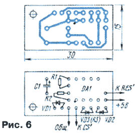
In Fig. 6 shows a drawing of the PCB.
Literature
Author: D. Nikishin, Kaluga