


")

The author of published articles alterations improve playback the image on the TV screen.
In Russia and other post-Soviet countries in operation is still many TV brands "Horizon", "knight", "the Seagull", "Youth" of the third to fifth generations. They applied a standard video channel on the chip K174XA33(TDA3505) and transistor amplifiers. With the aim of improving the quality of the image the screens of these TVs at first proposed to slightly modify (simplify) them the video amplifiers, although objectively it degrades to some extent view signal.
To illustrate the proposal, consider the simplified schematic diagram shown in Fig. 1, a single channel amplifier, the most widely used in TVs brand "Horizon". Especially should pay attention to the transistor VT3. It serves to reduce the output resistance of the amplifier and ensure high speed recharge parasitic capacitance that exists in the tube between the electrodes of electron guns. From the point of view of signal amplification this is absolutely the right decision. However, from the point of view of perception image it seems not straightforward.
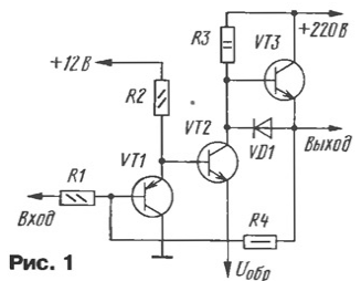
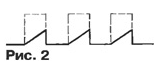
Consider what happens if you remove the VT3 transistor instead of a diode VD1 install the jumper. Obviously, then, because of an increase of the output resistance will have distortion of the video signal on the fronts of the pulses. At the same time, these distortions will be perceived differently, depending on the current recharge parasitic capacitance. At a voltage of 180 V on the resistor R3, the resistance is 18 ohms, the current recharge is equal to 10 mA, and when voltage 18 V does not exceed 1 mA. However, if the amplifier is supplied the signal of small amplitude relatively high frequency forms meander depicted in Fig. 2, the dashed line, at a level of the constant component of the signal will be reinforced with virtually no distortion. At low DC component it will turn into a sequence of triangular pulses (flat front and vertical recession) very small amplitude, shown by the solid line.
It should be reiterated that, from the point of view of fidelity signal amplification is bad. However, for the viewer this means reducing the visibility of small signals (and, first of all, noise) at levels close to the black level. Emerges the effect of noise reduction in the amplifier. Recall by the way that the principle of negative modulation of the radio signal broadcast also serves to reduce the visibility of weak interference, since they are below the black level.
In addition to the above, it should be noted that the emitter junction the VT3 transistor and diode VD1 are in the chain of General feedback (OS) amplifier and during the pulse edge signal that there is a gap circuit OS. The result is due to the phase delay signal OS have distortion the switching nature in the form of surges. In the amplification video signals of high frequency such indeterminate state amplifier it becomes very noticeable. On the screen that appears as distortion of the drops brightness (for example, difficult to read the credits on a black background at the end of the film).
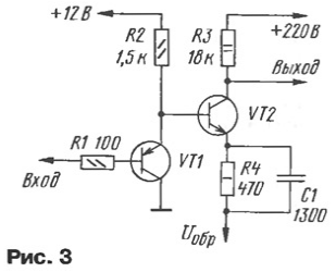
Schematic diagram of the amplifier, which takes into account the stated above the considerations presented in Fig. 3. It allows with minimal alterations to use existing video amplifiers. General OS replaced by a local. The selection resistor R4 can change the gain of the amplifier, and the selection of the capacitor C1 to achieve the most optimal for perception correction definition image. Additionally it is necessary to reduce an exemplary voltage up to 2,5…3 In (common for all amplifiers), which reduce the resistance of the resistor, connected between the base and the collector of the transistor in the cascade forming the LRA voltage.
Consider, for example, a specific revision of the TV "Horizon 51CTV441". A fragment of its concept is depicted in Fig. 4. Changes are shown for amplifier red (R) channel, modify the other two similarly.
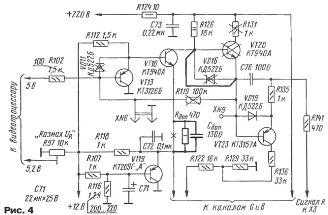
First of all, remove the diode VD11, the transistor VT20 and resistors R119, R131 (marked with a cross). Instead of the resistor R102 resistance 1.5 kω set resistor 100 Ohm, and diode instead VD16 - jumper. Further rip (cut) printed conductor connecting smithery transistor VT16 and VT19. Way surface mounting solder in the gap parallel-connected resistor Rдоп impedance of 470 Ohms and a capacitor Clim capacitance 1300 PF is Most convenient to do this, using the items for SMD size 1206 or 0805. They can be soldered directly on the incision site. To reduce model voltage resistor R116 resistance 1.2 ohms replace the resistor resistance 200…220 Ohms.
In other models of TVs may be some differences between the video amplifiers, associated, typically, with chains of high-frequency correction. Resistor R3 (see Fig. 1; in Fig. 4 - R126) may have a nominal value of 24 ohms. In this case, it must be reduced to 16…18 ohms.
Once finalized, the TV screen colors to become more saturated and evenly spread during the transmission of the dominant color of the effect denoising the signals of non-primary colors are suppressed. The image becomes in somewhat idealized.
Finally, it is possible to improve the image quality on these TVs, replacing submodule correction color transitions SCC-45 to the delay line LSAM-0.47 in chains the luminance signal. The inputs color-difference signals R-Y and B-Y needs to connect with corresponding outputs.
The fact that the increase of the slope of the differential color-difference signals at all the usefulness of such a function does not create a significantly noticeable visual effect improve your image. The same delay for the luminance signal Y in the chip, first, significantly reduces the quality of the signal and therefore of the picture, and secondly, limits the scope of the luminance signal at the input of the video processor HAS that turn implies the limitation of the dynamic characteristics of the image.
A schematic diagram of one embodiment of the node delay for the luminance signal presented on Fig. 5.
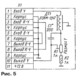
The capacitor C1 is select for the best quality image in the range 100…300 pF. Rigged resistor R1 sets the level of the luminance signal such that the brightest image has not yet appeared whitish areas.
The delay line must be LSAM-0,47-1150 or similar (almost "cube"), which used in TVs "Youth" models TC/312. All elements of the node placed on an extra Board, so that if necessary it was possible to restore the standard configuration of the TV.
Author: Sergei Kostitsyn, Izhevsk