


")

Remote control (RC) can be used to enable and turn off the lighting in the room where the TV is. The author suggests the chandelier with the decoding of the commands used. If decoding produce, as is sometimes done, the lighting in the management of the TV can be switched randomly.
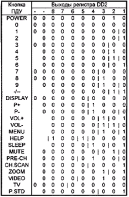
The encoding of the commands used by manufacturers in the distance control TVs, are quite diverse. In most cases, the team is transmitted as a sequence of several (ten or more) packs of pulses different durations, and information are not only the pulse, but the pause between them. For example, the TV remote control SK-3338ZR SAMSUNG contains 11-13 bundles, each of which consists of 32 or 64 pulses with the frequency of filling of about 40 kHz. The duration of gaps between impulses corresponds to 32 or 64 periods specified frequency. A long press on the button command of the parcel are repeated with a frequency of about 9 Hz. The first three packs packages do not depend on the transmitted command, but for odd and even taps on buttons they are different - or short-long-short or short-short-long.
Command codes the remote control above the TV shown in the table. It applied the following designations: "0" - short stack; "1" - long tutu; "|" - long pause. A short pause is not specified, as in all cases between bursts is any pause. The present part of the commands that follow the first three packs, they contain from 8 to 10 packets of pulses. In the table these bundles aligned ends - so, after taking they are arranged in a shift register of the receiver commands.
The author developed the device, decrypts the SLEEP command, it shows in Fig. 1. The signal from the infrared photodiode VD1 increases specially designed for this chip DA1 in stewkley. its release (vivod) packs of pulses of positive polarity (Fig. 2) is input to the node, collected on elements VT1, R1, R2, C6, DD1.1. This node transforms them into single pulses, the length of which is slightly greater than the length of the bundles [1]. The use of the transistor VT1 is normal for this node of the diode reduces the load on the chip DA1.
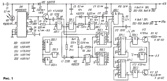
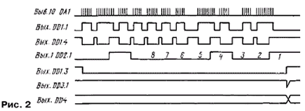
The pulses from the output of the element DD1.1 are inverted by the element DD1.2 and the differentiating circuit С7R3 arrive at the single vibrator on the element DD1.4 and run it. The pulse duration of the low level at the output of single-shot - about 1.2 MS, which corresponds to the sum of short and long durations packs. The decay of the pulses from the output of single-shot (a drop in the levels of the log. 0 log. 1) recording information from the exit of the element DD1.1 in the first digit shift register DD2.1 and DD2.2 and shift it in the direction of increasing numbers outputs. If the next accepted packet was short, at the end of the the single-shot pulse at the exit of the element DD1.1 the present level of the log. 0, which will be written into bit 1 of the register. Accordingly, when a long bundle the output voltage of the element DD1.1 corresponds to the log. 1, it will be recorded in the register. As a result after the command has been accepted in the register DD2.1 and DD2.2 is formed information about its last eight bundles, and on the last - in the discharge 1. The voltage at the output circuits when receiving the SLEEP command is shown in Fig. 2 - in bits 1 and 4 of the register - log. 1, and the rest of the log. 0. Information about duration of pauses at one of these events is lost.
The node on the element DD1.3 operates similarly to the node on the element DD1.1 - while on the exit of the element DD1.2 pulses are low level, the output DD1.3 - the level of the log. 0, after the team on it with a slight delay appears high logic level. This level difference is differentiated by a chain С12R8 and in the form of a pulse of positive polarity is input to the element DD3.1 AND-NOT. If adopted selected, this element is triggered at him the output is formed by a short pulse of low level, switching to a new the state of a chain of triggers DD4.1 and DD4.2. The signals from the outputs of control the passage of pulses corresponding to the moment of transition of the mains voltage through zero and applied to the input of element DD5.2. With his exit through the elements DD5.1 and DD5.3 and the transistors VT2 and VT3 those impulses are sent to the control the electrodes of the triac VS1 and VS2 (Fig. 3). In the anode circuit of the triac is enabled the lamp HL1-HL3 lighting chandeliers. When multiple command SLEEP switches one lamp HL1, two lamps HL2 and HL3, or all three lamps, then they all go out. The same result is obtained when contacts the micro switch SB1. Elements R9, R10 and C13 suppress contact bounce and protect the element DD3.1 overload.
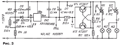
It is shown in Fig. 3 the node of the power supply and pulse forming network, launching triacs, is somewhat different from that described earlier by the author [2]. Instead of one of diode half-wave rectifier there is a Zener diode (VD5), and control electrodes of the triacs are served impulses fairly long duration - about 0.75 MS, which corresponds to the middle point of the transition network voltage through zero. The current supplied to the control electrodes during action of pulses is about 80 mA, which is sufficient for reliable the rectification characteristics of triacs and Bespalova their inclusion in the beginning each half period.
When the above duty cycle of the pulse current is consumed for simultaneous the inclusion of the two triacs, an average of about 12 mA. This current is quite can provide a dampening capacitor C14 node power capacity 0.68 UF. The pulsed nature of consumption of the main part of the current leads to large the ripple voltage on the filter capacitor C15. Their smoothing provides integral stabilizer DA2. It's cheaper than, for example, the use of capacitor C15 is twice larger capacity.
The lighting device is assembled on two printed circuit boards made from a two-sided foil fiberglass 1.5 mm thick (one - the circuit elements of Fig. 1 on the other (Fig. 3). Boards are designed for mounting in the housing switch-"dergalki" that are installed in homes near the ceiling.
DA1 chip together with its related parts for protection against electric the covered pickups soldered at several points the screen is made of thin copper.
Micro switch SB1 is provided with a lever which was cut from organic glass. On his the thin end of the fixed string, pulling which you can control inclusion chandeliers manually.
In your device, you can use the IC series C, K, KR, DD3 interchangeable the chip LA these series. Transistor VT1 - any low-power silicon the structure of n-p-n current transfer ratio base h21e not less than 100, transistors VT2, VT3 medium and high power with h21e at least 80 at a current collector 100 mA. The transistors VT4 and VT5 - almost any silicon low-structure p-n-p. The triac VS1 and VS2 series CU in plastic the case with the indices B1, C1 or D1 or TC-106-10 at a voltage of At least 400 (the index after the specified designations to 4 or more).
Diodes VD2-VD4, VD6 - any low-power silicon, Zener VD5 - on the 12 V working current less than 20 mA.
As a chip of DA2, you can use any domestic integrated stabilizer for voltage-6V - KREN, KREN or import 79L06, 79M06, 7906, with any prefixes and suffixes.
All resistors - MLT corresponding power capacitors - km-5, km-6, K73-16 (C14) and K52-1B. In place of capacitors is possible to install K50-35 or their imported counterparts.
Configuring the device is recommended in the following order. First on Board with details on the scheme of Fig. 1 the inputs of the element DD5.2 to connect with the General wire, and between the top (the scheme) in terminals of the resistors R11 and R12 and chain +6 In to turn on any led. After that, the contacts "+6" and "General." Board it is possible to apply a voltage of 6 V from a lab power supply.
Pushing the rod micro switch SB1, you should make sure to alternately turn on and off LEDs. Feeding the SLEEP command from the remote control at the photodiode VD1 (with distance 0,5…1 m and not a very bright light), you need to check the clarity operation of the device and if necessary to select the resistance of the resistor R4 for receiving duration is generated at the output of a single vibrator on the element DD1.4 pulses in the range 1,1…1,3 MS. This work is better done using oscilloscope with triggered sweep. In its absence, can be put in place R4 variable resistor of 220 ohms in series with the restrictive resistance 51 ohms to determine resistance range in which is provided by the reception team. After that to the place of R4 should be set a resistor with a resistance corresponding to the middle of this range.
To check the card with the PSU (according to the scheme of Fig. 3) between its contacts "+6" and "General." we need to solder in a resistor 510 Ohm any power, connect the Board to the network and, being careful (and all its components are at mains voltage), to measure the voltage between the common wire boards and circuits "+6" and "-6V". If they differ from nominal not more than 0.5 and 1 V, respectively, the boards can to connect and test the operation of the device in Assembly with a load in the form lighting bulbs.
Literature
Author: S. Biryukov, Moscow