


")

To successfully repairing electronic equipment, in particular TVs, it is necessary to imagine the work units device, know the meaning of their elements. For example, switching power food cause usually great difficulties in the repair. Published here the article author talks about the power module MP-403 applied in many models of TVs.
TV power module MP-403 was already considered in [1 and 2] with different level of detail. However, in [1] is not quite accurately described the process of running the module and not told about it mainly the oscillatory regime (a link to the module MP-1). In the book [2] from the entire startup process is actually explained only feed opening voltage to the base of switching transistor VT9, and further it is argued that the processes run proceed the same way as in module MPZ-3. The basic self-oscillating mode of operation is also not mentioned. Meanwhile when Troubleshooting pulse in the power module, it is very important to know the work in these two basic modes. Unfortunately, the outline of schematic diagrams in both publications is that to use it is inconvenient.
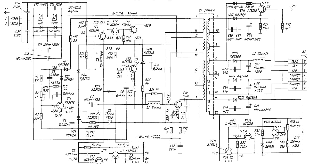
In the present paper an attempt is made to remove these gaps, i.e. to describe the module at startup, established in the oscillatory regime in the case of short circuit to explain the purpose of individual components and assemblies, as well as to give a "readable" concept. She is depicted in the figure.
(click to enlarge)
Starting device module is assembled on the transistors VT4, VT6 and VT7. The last two directly provide the launch, and the first is used to turning them off when the transition module in self-oscillating mode.
After turning the TV on capacitor C9 begins to charge (through the elements R19, VD4, R14, R16) pulsating voltage generated from the rectifier the diode VD7. Until the voltage on the capacitor C9 is small, the transistor VT4 is closed. The transistor VT7 is opened by the base current flowing through the resistors R28, R25, R14, R16. On the emitter junction of transistor VT9 opening voltage comes through resistors R28, R14, R16, the transistor VT7, the emitter junction of transistor VT6 and the winding 5-3 of the transformer T1. The transistor VT9 starts to open.
Through the winding 19-1 transformer flows linearly increasing current, which induces in the coil a positive feedback (PIC) 5-3 EMF of mutual induction. Current the base of the transistor VT9 generated by the winding of the PIC, passes through the elements R27, VD11 and VT6. The collector current of the transistor VT9, flowing through resistors R14 and R16, provides them the mounting tension.
After reaching a certain value, the voltage across the resistors R14, R16 through the chain C5R11 (charging the capacitor) opens SCR VS1. Last through the inductor L1, uncharged capacitor C7 and resistors R14, R16 emitter shunt the transition of the transistor VT9, closing part of the current winding 5-3 transformer itself. As a result, the currents in the base and collector of the transistor VT9 decrease, the voltage at the winding 5-3 reverses, transistor and SCR are closed.
The secondary transformer windings have a voltage impulses that begin to charge the capacitor filters the secondary rectifiers. Since the currents charging large (almost a short circuit mode), the voltage on the secondary the windings and the winding of the PIC (5-3) are small and disappear quickly. In other words, the energy windings is rapidly transferred to the uncharged capacitor.
Again the current is run through the emitter junction of transistor VT6 is opened the transistor VT9, feasting upon the then current winding of the PIC opens and SCR closes the transistor VT9 and myself. Consequently, there is some number cycles on and off of the transistor VT9, during which the capacitors S, C31, C32, C34, C35 secondary rectifiers are charged to voltages close to the nominal. Currents recharge them take the form of pulses, exponentially declining to zero, allowing you to get the module from short circuit mode.
By this time, the capacitor C9 can be charged up to the voltage of opening transistor VT4. Its collector current increases the voltage drop across the resistor R28 and closes the transistors VT7 and VT6 the start device. Module goes in self-oscillating mode of operation in which already loaded capacitors C5, C7 (through the diode VD6 from winding the PIC) and C8.
In the steady state when the lid of the transistor VT9 linearly increasing current flows through it as when you run. Resistors R14, R16 is created the same in the form of a voltage, which is algebraically with the voltage the capacitor C5 and through the divider R11R13 acts on the control electrode the SCR VS1. While the amount of stress becomes positive and exceeds a certain value (about 0.6 V), the latter is closed. Voltage winding 5 PIC - 3 generates the base current of transistor VT9 through the resistor R20 and the transistor VT5, maintaining the transistor VT9 open.
The transistor VT5 serves as a node is proportional to the base current control transistor VT9. In addition, through him, charging the capacitors C5, C8 and occurs the opening of the transistor VT9. In the steady state, the transistor VT5 is open the voltage of the capacitor C5, is applied through resistors R17 and R20 to it the emitter junction.
Increasing the voltage with resistors R14, R16 through the elements and R20 C8 affects the emitter junction of transistor VT5, proportionally reducing it the resistance through the base current of the transistor VT9 that provides approximately constant degree of saturation of the transistor VT9 current increases his collector. When the collector current of the transistor VT9 increases to around 3.5 And, the sum of the voltages across the resistors R14, R16 and capacitor C5 becomes sufficient for opening the SCR VS1. Through it, the inductor L1 and the resistors R14, R16, the voltage on the capacitor C7 is applied in closing the polarity to the emitter junction of transistor VT9. The discharge current of the capacitor is directed counter to the current of the base of the transistor and higher than the last. The transistor VT9 very quickly closes the discharge circuit of the capacitor C7 through the SCR is interrupted, the current of the latter decreases, causing it to close.
The collector of the transistor VT9 and the windings have a voltage pulses through winding currents flow that recharges the capacitors filters. Decreasing, they induce in the winding 5-3 voltage of the PIC (plus at pin 5). It opens the collector junction of transistor VT5 through resistor R17, diode VD5 and the inductor L1. As a result, the transistor VT5 is opened in the opposite direction. The current charging of the capacitor C5 flows through the transistor and the elements R20, VD5, L1. At the same time recharges the capacitor C7 through the diode VD6 and the inductor L1) and C8 (through the collector junction of transistor VT5 and resistors R14, R16, R26).
Voltage POS winding 5-3 transistor VT9 is maintained in the closed state through the open in the reverse direction, the transistor VT5 and a resistor R20.
When charging currents of the capacitors of the filters of the secondary rectifiers are reduced to zero, the voltage across winding 5-3 also becomes zero. At this point the voltage of the capacitor C5 opens the emitter junction of transistor VT5 via resistors R20 and R17, opening the transistor in the forward direction. At the same time the voltage of the capacitor C8 passes through the collector junction and the winding 5-3 on the emitter junction of transistor VT9. When this occurs the initial base current last and again starts increasing its collector current under the action of PIC.
In the mode of short circuit in the secondary circuit when closing the transistor VT9 all accumulated transformer T1 magnetic energy is absorbed by the circuit, closing the secondary winding. The load current decreases much slower than in normal mode, resulting in the coil POS 5-3 transformer almost stops induced EMF (plus at pin 5). This not only causes termination of charging of the capacitor C8, but even his recharge in return the direction of the voltage of the capacitor C5 through the resistor R14, R16 and R17.
Since the transistors VT6, VT7 start device closed permanently saturated transistor VT4, the transistor VT9 has no voltage source for initial opening, and even, on the contrary, is closed the voltage of the capacitor C5 through the resistor R17, the collector junction of transistor VT5 and winding 5-3 the transformer T1.
Therefore, unlike in module MPZ-3, which in the short circuit works in the regime of short pulses, the module MP-403 is completely off. So if the power module was turned off by the artificial node short circuit the elements VD16, R31, VT11, then the timer needs to be unloaded capacitor C9. To do this, unplug the TV from the mains and then on again to turn on after 5…10 seconds.
The appointment of nodes and elements of the module:
- VD7-VD10, C10-C13, C17, C18 - voltage rectifier network;
- VT1, VD3, C2, VD1, R5, R1-R3, C1, R7, C4 - node output stabilization voltages;
- VT2, VT3, R9, R6, R4 - device surge protection for faults in site stabilization;
- VT11, R31, VD16 - node create artificial short circuit to disable module fault-line scan (module MP-403) or by the signal from the control unit;
- VT13-VT15, VD18, R33, R34, R37 - R39 - voltage regulator +12 V;
- VT9 - power pulsed transistor switch;
- VS1 - SCR torque control closing of the transistor VT9;
- C7 - capacitor for closing the transistor VT9 through an open SCR (it should be indicated that during startup, the current through it flows in the opposite direction to its passport polarity that is necessary to consider when evaluating its reliability);
- VD6 - switching diode to charge the capacitor C7;
- C5 - capacitor to generate a negative voltage bias on the control the electrode of SCR;
- VD5 - switching diode to charge the capacitor C5;
- VD4 - diode, used to make when you start charging current of the capacitor C9 is not passed through the control electrode of SCR VS1 and is not charging the capacitor C5 in the opposite direction;
- C8 - capacitor for the initial opening of the transistor VT9 in self-oscillating mode, is included along with the elements of VT5 and R20 in the proportional control node the current of the transistor VT9;
- VT5 - switching transistor of a node is proportional to the base current control transistor VT9, provides charging capacitors C5 and C8;
- R14, R16 - resistors current sensor transistor VT9.
The action of the protection device module is described in detail in [1], [2], and the work site stabilization in the oscillatory mode at rated load and at idle the move did not differ from those applied to similar devices in the module power MPD-3.
Literature
Author: I. Molchanov, Moscow