


")

Among the Amateurs become increasingly popular work in the broadcast low power QRP. Especially attractive is the fact that the apparatus for QRP can be performed entirely on the transistors and to feed from a low voltage source.
Broadband power amplifier, the circuit of which is shown in the figure, provides linear amplification SSB and CW signals in all LW bands. The power supplied to the terminal cascade at a voltage of 12V exceed 10 W, which corresponds to the international definition of QRP equipment.
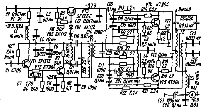
The signal from LW exciter (transceiver) flows through the emitter-follower (transistor VTI) on the pre amplifier operating in mode A (transistor VT2). The input impedance of the next stage of about 10 Ohms, therefore, to harmonize it with the advanced broadband amplifier is applied to the transformer T1 with a conversion ratio of 4:1 (impedance). Capacitors C and C13 equalize the amplitude-frequency characteristic of this stage.
Push-pull output stage (VT4, VT5) works in AV mode. To the load it is connected through a broadband three-winding transformer T2 with a conversion ratio of 1:1. This transformer allows you to prevent the saturation of the magnetic circuit DC component of the collector current. Constant quiescent current of the output transistors is supported by the stabilizer on the transistor VT3. Diodes VD1 and VD2, which sets the bias voltage of the transistors VT4 and VT5, are in thermal contact with the heat sinks.
When establishing the first cut off the amplifier output stage, the secondary winding of the transformer T1 is loaded by two series-connected resistors on the 8.6 Ohms, and the point of its connection connect to GND. The selection of resistor R2 sets the quiescent current of the transistor VT2 (~100mA). Then the input of the amplifier serves high-frequency voltage. In normally functioning pre-amplifier with an input voltage of 220 mV limit signal in the collector circuit of the transistor VT2 should occur at the level of 9 V, and the amplitude of the signal at each of the terminals of the secondary winding of the transformer T1 (referenced to GND) should be about 1.1 V.
Then, the emitter of the transistor VT3 is connected to GND via a resistor 17 Ohms and adjusted by the resistor R6 is set at the output of the voltage stabilizer 0.75 V. Restoring circuit of the output stage and connecting the dummy load (resistor of 50 Ohms and a power dissipation of 5 W), turn the power on and the same resistor R6 sets the total quiescent current of transistors VT4, VT5 is 40 mA.
The limitation of the output voltage should occur at the level of 22 In, and consumed terminal cascade current should be in the range of 0.7 to 0.8 A.
One of the criteria of sustainable (without excitation) of the power amplifier is smooth, without abrupt changes, the current increase. quiescent output stage, with increasing excitation RF voltage.
Transistors SF137E and SF126E can be replaced respectively by CTV and CTB, and diodes SAY12 - KDA.
Literature
- DоЬerenzг W. Eine einfache 10-W-QRP-Endstufe fur Kurzwelle.- Funkamateur, 1984. No. 2. S. 89-91.
Publication: N. Bolshakov, rf.atnn.ru