


")

To improve the range and quality of radio communication within the ranges on УSW radio stations often use antenna amplifiers. Their main purpose increased sensitivity of the entire receiving path and compensation of losses signal in the feeders.
In Fig. 1 shows a diagram of the antenna amplifier band 1296 MHz. He collected low-noise bipolar microwave transistor. Input and output of the amplifier is installed selective circuits L1C1 and L3C9 based on half-wave resonators. To protect transistor from the powerful transmitter on the inlet and outlet of the cascade set suppressor diodes VD1-VD4.
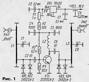
Mode transistor DC current is given resistive voltage divider R3, R4 and load resistors R1, R2. At the collector is installed recommended for this type of transistor the supply voltage is 7 V. Rigged resistor R1 can be changed the current of the transistor in the range of 1…10 mA. Food the amplifier is stable with an integral voltage regulator on a chip DA1.
The device incorporates the following types of items: fixed capacitors Leadless K10-17B or similar imported, rigged capacitors - PDA-MT capacity 2…7 pF, lock capacitor - K10-51, B7. Rigged resistor - SDR-19, constant - P1-12, P1-4, IFL.
Specified in the diagram, the transistor can be replaced by CTA-2, CHA-2, TA-2, chip stabilizer - CREA or B.
Resonators L1, L3 made of strips of copper foil (preferably silver-plated) thickness 0.2…0.4 mm, a width of 5 and a length of 58…60 mm. Strip of-· in libalsa a U-shaped bracket length 48…50 mm and a height of 4…5 mm, both ends of which are soldered to a common wire of the circuit Board. The coil L2 is wound wire Sew-2 0,2 mandrel with a diameter of 3 mm and contains 6…7 turns.
Most parts of the amplifier is placed on a printed circuit Board made of bilateral foil fiberglass 1.5 mm thick. Sketch of the working side of the PCB and the location of the main elements shown in Fig. 2.
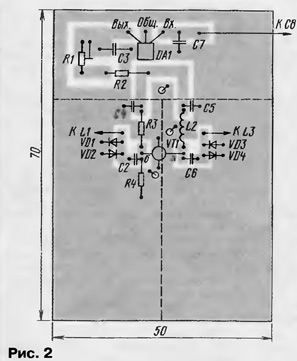
Foil on the second side of the Board used as a screen. In the circuit Board made several openings which are connected by soldering between the screen and the overall wire working. The design of the amplifier shown in Fig. 3, and build it should be in a certain order.
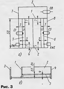
First mounted on the circuit Board, all parts, except loop and tuning capacitor, RF connectors, as well as resonators L1, L3. The fee is the Foundation on which is then soldered to the Central partition 1, 2 and side walls 3, 4. In the partition wall 2 is cut under the transistor. The following solder resonators L1 (5), L3 (6). In the last turn to the Board solder (also with two sides of the Board) side walls 7, 8 RF jacks and capacitors C1, C9. The capacitors, in turn, is brazed to the means resonators L1 and L3 respectively. All necessary installation dimensions also it is shown in Fig. 3.
The establishment of an amplifier is reduced to the input and output circuits, the center frequency of the range of trimmer capacitors C1 and C9. Input the impedance of the amplifier, and hence its CWS can be changed by selecting a point connect the center conductor of the socket XW1 to the resonator L1. Rigged resistor R1 sets the desired current through the transistor. Scelti it on the hearing for the best reception of weak signals, however, be aware that this will change somewhat and SWR of the amplifier. The setting should be repeated several times. To improve the stability of the amplifier in the collector circuit transistor can be set small resistor (P1-4, P1-12) resistance 5…10 OHM.
Tuned amplifier close the top cover, made of tinplate. To protect from moisture rigged capacitors, as well as all the joints on the outside must be filled with an elastic sealant.
Collected by the author of the layout of the amplifier had the following parameters: gain -11 dB bandwidth -3 dB bandwidth is about 20 MHz, the input VSWR is not more than 1.2.
Instead of the transistor can be applied monolithic arsenicalis chip MGA86563 (Nechaev I. "Antenna amplifier UHF on-a-chip". Radio, 1999, No. 4, S. 8, 9) by turning it, as shown in Fig. 4.
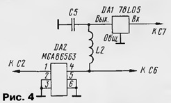
The gain of such the amplifier will be in the range 18…20 dB, and the noise factor is not more than 1.6 to 1.7… dB. Accordingly it is necessary to adjust the topology of the PCB.
Author: I. Nechaev (UA3WIA)