


")

The apparatus is designed to enable (disable) and protection against overcurrent various electronic equipment, lighting and other appliances with mains power supply. As a switching element is equipped with a high field switching transistor.
Currently part of electronic equipment - TVs, DVD players, some equipment for computers - no special network power switch and is connected to the network, although this is not necessary. Along with the fact that this wasted electricity, increasing the likelihood of system failure due to emergency situations in the network. The proposed device can be applied not only to include such equipment, but also protection against overcurrent.
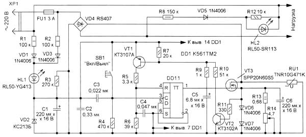
Switching load is a powerful field switching transistor VT3, which is included in the diagonal of the diode VD4 rectifier bridge. In the circuit of the source of the resistors R13, R14, performing the functions of the current sensor. Diodes VD6, VD7 limit the voltage on them, and the capacitor C6 suppresses the impulse noise. Varistor RU1 protects the VT3 transistor from breakdown of the spikes that occur in the network when switching inductive loads. The control node of the switching transistor is built on transistors VT1, VT2 and D-trigger DD1.1, which is included as a frequency divider by two. Power supply node is supplied from the rectifier diodes VD1, VD3 with damping resistors R1, R2 and parametric voltage regulator Zener diode VD2, capacitor C1 is a smoothing.
HL1 led indicates the presence of mains voltage on the input device. If the power load is turned off, the current through the led HL1 increases, so the brightness of its light increases. The load is connected in series with the diode VD4 bridge, overload it, as the device itself, protects fuse FU1. Led HL2 indicates the presence of mains voltage on the load. The resistor R12, shunt led HL2, it eliminates a faint glow that can occur due to the reverse current of a field effect transistor VT3 and the current through the varistor RU1. After the filing of the mains voltage on the D-flip-flop DD1.1 receives the supply voltage. The capacitor C5 is designed to generate pulse setup D-flip-flop DD1.1 in the zero state with a low voltage logic level on the true output (pin 1 DD1.1). It happens so. At the time the application of supply voltage charges the capacitor C5, the transistor VT1 is opened and the input R (pin 4) D-flip-flop goes to a high level.
Field-effect transistor VT3 is closed and the voltage on the load is not supplied. When you short press the SB1 high voltage level is received at the counting input of D-flip-flop, and it will switch to a state with a high level of the direct output. The channel resistance of the transistor VT3 is reduced to a fraction of an Ohm, and the load will receive the supply voltage. Subsequent press the SB1 will toggle the D-flip-flop in the low state, the direct output, the transistor VT3 is closed and the load will be de-energized. If you increase the current consumed by the load increases the voltage on the resistors R13, R14, and when it reaches 0,55…0.6 V, the transistor VT2, followed by VT1 and will begin to open, the input R of D-flip-flop goes high level, and he switches to the low state, the direct output, so the transistor VT3 is closed and the load is de-energized.
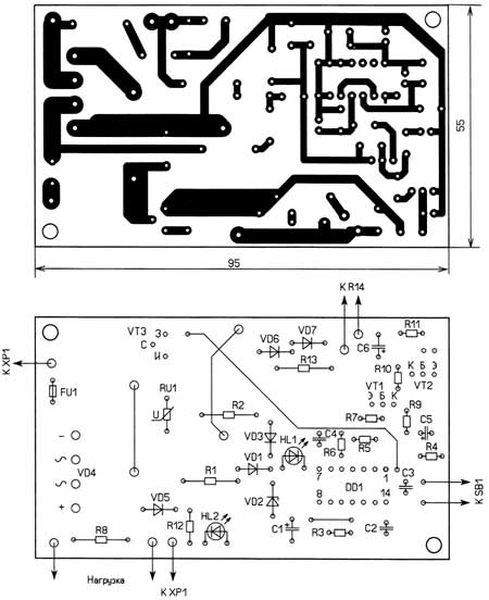
Current protection operation can be set by resistor R14 in the range of 0.08…0,36 A. Since in the steady state, the transistors VT1, VT2 closed, and the D-flip-flop consumes low current, after disconnection of the mains voltage the capacitor C1 may be a long time to save battery. For his discharge is a resistor R3. This can be useful if you want the long (minute or more) mains voltage, the load was disconnected. Most parts are placed on the PCB of one-sided foil fiberglass, a drawing of which is shown.
It is designed for the use of fixed resistors MLT, S1-4, S2-23 (variable wire wound resistor PPB For installing on the wall of the plastic housing), oxide capacitors K50-35 or imported, other - K10-17. Varistor TNR10G471К to replace FNR-10K471, FNR-07K471, Zener XB - XA, 1N4743A, a diode bridge RS407 - LWL08, LWL10, 1N4006 diodes - 1N4007. LEDs you can apply constant but different colors of light (HL1 - green, HL2 - red) of the series L-53, CIPD. Transistor KTA you can replace any of the series CT, KT361, CT, transistor KTA - any of the series KT315, KI3102, CT, but you must pay attention to the difference in cocalico transistors. Field-effect transistor SPP20N60S5 has a resistance of the open channel to 0.19 Ohms, the maximum voltage of the source-drain 600 V, maximum drain current 20 a, And the pulse - to 40 A. His closest analogues - IRFP460, STW20NB50, but you can set up more powerful - SPW47N60C3, with the resistance of the open channel of 0.07 Ohms and the maximum drain current 47 A.
In the experiments or to operate the device with a low power load will approach the IRF840 MOSFETs or series K, K. Button SB1 - any small-sized with a long plastic pusher, for example, TD06-XEX, TD06-XBT. When specified on the diagram the values of resistors R13, R14 to the device you can connect a load capacity of up to 75 watts. So when you connect to a device, such as an incandescent lamp power 100… 150 W, current protection works and won't give it to to include.
To run a more powerful load, it is necessary to reduce the resistance of the resistor R13. Peak value of current protection operation can be found from the expression Ia = (0,55 0,6…)/(R13+R14). Most electrical and radio devices with its inclusion in the network consume the so-called inrush current exceeding the rated several times. When overcurrent has not worked, in parallel to the emitter junction of transistor VT1 need to install oxide capacitor (positive output to the emitter) with a capacity of 47 to 100 UF. The seat for this capacitor on the Board has.
Inrush current devices with switch mode power supplies having input capacitors with large capacitance, can be reduced by including in series with the load wirewound resistor to 3.3…of 5.6 Ohms and a power of 5-10 watts, for example, C5-37, C5-16. If this is not done, then a relatively low-power field-effect transistors (IRF840, etc.) can be damaged even after the first switching of the load (TV, printer, monitor)
Author: A. L. Butov, S. CORBA, Yaroslavl region; Publication: www.cxem.net