


")

Table clock, which tells this article, differ from many similar structures in that they have not applied luminescent, and large led indicators. The alarm in this watch makes a two-tone signal with adjustable time and has an indicator the enabled state. In addition, the design provides damping insignificant zero on the scoreboard clock and power back-up time chip.
A schematic diagram of a clock shown in Fig. 1. To display the time in them used four large led display with common anode. In the experiments were applied CLCA, CLCV, CLCB with h = 18 mm and with CIPCA h = 25 mm. the basis of the hours themselves are integrated circuits CIE and CIE, described in [1, 2]. The elements DD1, ZQ1, R1, R2, C1 - C3 form a generator with a frequency divider, a DD2, VD3 - VD5, R5, C4 is the primary counter with elements management. The inclusion of these chips model. As the cathode decoder applied TTL chip KIT supplied from circuit +u pit via ballast resistor R9. Such inclusion is somewhat incorrect, as the input voltage for KID exceed in this case valid. But it has its advantage - from hours to remove the cathode keys (seven transistors with base the resistors).
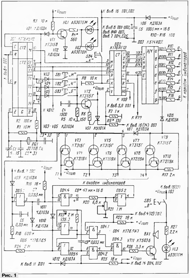
(click to enlarge)
Anodic keys made on transistors VT3 - VT10. The damping device trailing zero is simplified and contains only three elements - VD7, VD8, R17. Its action is based on fixing the ignition segment f, which is the hallmark symptom of digits 0 in relation to figures 1 and 2. When you see the output f of the decoder logic low level (less than 1 V) diode VD8 opens and shunt base current of the transistor VT9. The key on the transistor VT9. VT10 closes and extinguishes the indicator of tens of hours. As the dividing points dial used single LEDs HL1 and HL2, pulsing to the beat the second pulse.
Node disconnection indication contains the thyristor VS1 and the transistor VT2. In working mode VS1 kept open through the current supply chip DD3, the value of which is in the range of 30…40 mA. When an outage VS1 is closed, the chip DD3 from power disabled and indicators will extinguish. When further power is turned on, the thyristor VS1 remains closed and the numbers do not light up, although the separation point flash. It draws the user's attention and reminds him that after switching on hours their testimony should be coordinated according to a different clock (because it is unknown what the duration was a power failure). Turn on the display by pressing the button SB3 ("B"), wherein a pulse frequency of 128 Hz, which appeared on the base of the transistor VT2, decreasing them current and open the thyristor VS1.
The alarm made on chips DD4 and DD5 and works as follows. The pulses output from the HS chip KIA detected by circuit VD9R18C6, and negative differential voltage from the output of the element DD5.1 through a chain R19C7 starts the standby multivibrator elements DD4.4 and DD5.2. As a result the generator on the elements DD5.3, DD5.4 and its antiphase weekend signals control operation of the switch elements DD4.1 - DD4.3. In the end the base of the output transistor passes either the signal frequency 512 Hz (with the pin. 1 chip DD4) or 1024 Hz (with the pin. 5 chip DD4). Thus formed a two-tone signal, interrupted by pulses with a frequency of 1 Hz, flowing through the resistor R24. The switching frequency of the switch is determined the parameters of the elements R23, C9, and the signal elements R21, C8.
When specified on the circuit component values this duration can be changed from 0 to 60 C. Button SB5 performs the functions of a switch, the alarm, and the led HL3 - indicator is its enabled state. Diode VD10 blocks the delivery of a sound signal in case of false alarms the waiting multivibrator is not at a set time (for example, under the action of interference).
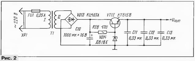
The hours power source consists of transformer T1, rectifier - VD13C10, and stabilizer voltage VT12, VD14, R28 (Fig. 2). His output a voltage of about 8.5 V, In the event of a utility power interruption circuits DD1, DD2 receive charge from capacitor C5, which is supported by the clock yet for some time (of course, without time indication). A number of elements hours in this mode eliminates leaks with outputs operating in chips disabled part time device.
Thus, the diode VD12 prevents leakage current through the pin. 5 chip DD4. Emitter the transition of the transistor VT1 is closed, the diode VD1, and the chip outputs CIE transferred to the high resistance state to the low logic level at the input V. Resistor R24 much resistance reduces the leakage through the pin. 8 and 12 chip DD5. All these measures make efficient use of energy the charged capacitor C5. The size of the last selected based on the expected the duration of the power failure. Experimentally when u pit = 9 obtained In such the time values of the conservation movement for the following sizes of capacitor C5:
- 1000 MK x 16 In (K50-16) - 5 min;
- 2200 MK x 25 In (K50-35) over 10 min;
- 6800 MK x 10 IN (PHILIPS) - more than 1 hour.
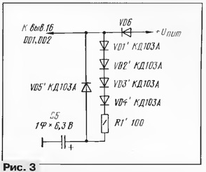
For longer power failures the use of a conventional capacitor becomes irrational, the best results have been obtained when using ioniser or a rechargeable battery. Capacitor 1 f x 6.3 In supports speed not more than 20 h (scheme C5 in this case should be changed in accordance with Fig. 3), and a battery of four elements D - 0.26 D - more than four days. In the latter case a watch is useful to complement the device automatic recharging of batteries.
Of course, all of these diets do not exclude the classical solutions applications battery "Krona" or similar.
The main parts of the watch are assembled on the PCB size 120x70 mm When mounting were used fixed resistors: KIM (R1) (it can be replaced with 2 - 3 the resistors MLT and MLT (other), variable resistor - SDR - 9a (R21). All oxide capacitors - K50 - 16, K50 - 33 or imported counterparts, C1 - KT - 25, the rest - ceramic K10 - 7 or km. Capacitors C11 - C13 soldered directly on the power pins of the ICS DD1, DD2, DD4. As transistor VT12 you can use KT815, CT; and transistors VT4, VT6, VT8, VT10 - CT, CT, CT; the rest KT315, KT3102, CT with any letter indices. Transistor VT12 is fixed to the heat sink in the form of an aluminum plate size 15x25 mm. Zener diode VD14 - any small voltage stabilization 9…10 V for stabilizing current less than 20 mA (DB, DW, D (A - e, and others). Diodes VD1 - VD12 - any small-sized silicon. The thyristor suitable from CO. LEDs HL1 and HL2 choose the same color with digital indicators (and preferably one shade). The HL3 led to the illumination of any color. Used quartz resonator in the cylindrical body from the wrist hours. Dynamic head - any power of 0.5 or 0.25 W resistance the voice coil 50 Ohms. Perhaps the use of telephone primers TA - 4 (65 Ohms) and TC - HT - 67. Switches SB1 - SB5 - P2K, all of them are mounted on a common strap and button SB1 - SB4 without fixation, a SB5 with return re clicking. As the transformer T1 is used TP - 8 with damping resistor in the secondary circuit (MLT - 1 resistance 24 Ohms). Generally, you can use any small-sized transformer with a secondary winding voltage of 10.5…11,5 V At load current 200…250 mA (exceeding this voltage is undesirable because of the deterioration of the thermal regime in the watch).
In place of chips and DD4 DD5 can work similar from C. Decoder DD3 - KID in the body with plenary pin. Possible its replacement with a more affordable chip CRED in a plastic housing. On the schematic diagram (see Fig. 1) the numbering of all pins for this chip are in parentheses.
Clock setting is performed in such sequence. First, watch need to include in the network and make sure that when you press the button SB3 (B) stable activate indication. If not, the required selection of thyristor or replacing the transistor VT12 into another with high gain.
After that, the selection of the resistor R4 is necessary to set the desired brightness flashing the separation points (HL1 and HL2).
Then you should set an alarm. To do this, disconnect the diodes VD10 VD11 and and to test the standby multivibrator, the feeding level of the logic zero at pin. 12 chips DD4. Thus on the pin. 4 chip DD5 must be formed the negative pulse with a duration that depends on the position of the engine resistor R21. Further, the selection of elements R23 and R9 is necessary to set the switching frequency switch (within 6…12 Hz) in the most pleasant sounding the alarm, and the selection of resistor R27 is the brightness of the indicator HL3. This is followed by return diodes VD10 VD11 and in its place. If the duration of the sound signal alarm to not necessarily change, variable resistor R21 can be replaced the relevant standing.
In the next phase adjust crystal oscillator, using electron-counting the frequency (and the hours and frequency before measurement it is necessary to warm up for 1 h). First, the rotor of the capacitor C1 should be placed in the middle position and the selection of capacitors C2 and C3 to set the oscillation frequency is close to 32768 Hz, verifying it on the pin. 14 DD1 chip. Then the rotation of the rotor C1 achieve exact value of the frequency 32768,0 Hz. Fine adjustment is possible when measuring the period of oscillation on the pin. 4 DD1 chip (1) with a resolution of 0.1 MS.
In conclusion, the selection of resistor R9 should be set on the pin. 16 chip DD3 the voltage in the range of 4.75…5.25 V (of course, if you have enabled display).
And now a few words about a possible revision hours. In the described design was used, as already indicated, four types of indicators, but really good illumination is able to provide only devices CLTV. Alas, trouble many domestic indicators, especially large ones, is a big disparity in the glow within the segment and between adjacent segments, as well as significant the variation in brightness even at operating currents close to the maximum. One of solutions to this problem - the use of foreign indicators with common anode (single or dual), and a special four-digit time of Assembly. Crucial to this scheme, a separate output from each anode discharge, and for four assemblies and the ability to display time in 24 - hour format.
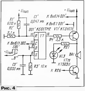
Another example of rework hours - the introduction of electronic alarm switch (Fig. 4). Thus from the old design removed the switch with detent, in you all can keep small buttons (IPP - 150 - 1 or the like). The alarm clock on any of the buttons SB1 - SB3 ("B", "H", "M") and can be switched off with a separate button SB1 ' ("In") installed instead of the SB5. After utility power interruption alarm is activated forcibly. (In Fig. 4 the newly introduced elements are numbered with the bar.)
It should be noted one drawback inherent in such watches, - low the contrast in strong external illumination. For this reason, desirable watch be placed in a darkened part of the room, avoiding contact with them direct the sun's rays.
The incorrectness of the output matching circuits DD2 with inputs DD3 it is desirable to eliminate. For this purpose the chips should install five emitter followers for any low-power silicon p-n-p transistors, for example KT361. Bases of the transistors should be connected to the outputs DD2, the emitter - to the corresponding inputs DD3, collectors - to GND.
Literature
Author: Dmitry Nikishin, Kaluga