


")

K. Smolyakov from Nizhny Novgorod, took the repetition of regulators the description in [1], has managed to combine in one device and two to create the device capable of handling supplied to the load power as by changing the number the "active" half-periods of the mains voltage, and pulse-phase method.
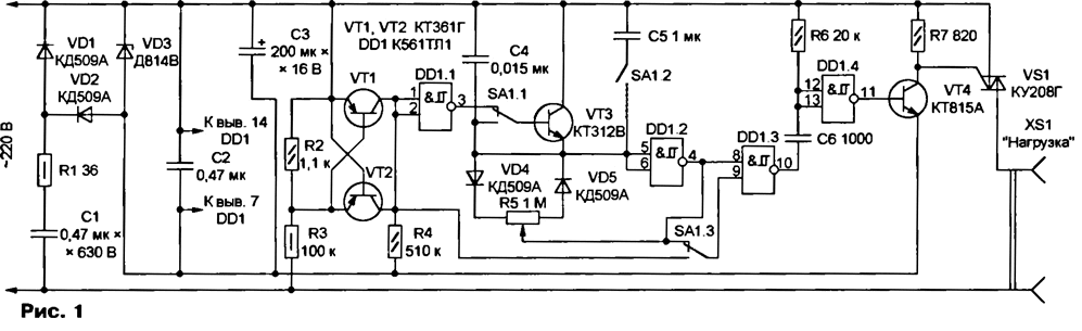
In his the regulator, assembled according to the scheme in Fig. 1, only one chip DD1. Mode work change the switch SA1 with three groups of contacts (used the band switch from a portable transistor radio). The node power (diodes VD1, VD2, the Zener diode VD3), driver "zero" pulses (transistors VT1, VT2), output node (differentiating circuit C6R6, element DD1.4, the transistor VT4, triac VS1) remained the same as in the prototype.
(click to enlarge)
Consider the operation of the device in the mode of power control the phase of the pulse method (switch A are shown in this position). The pulses from the output of the element DD1.1, coinciding with the moments of transition network voltage through zero, open the transistor VT3, when the instantaneous value the mains voltage is close to zero. As a result, the capacitor C4 discharges through the transistor and the voltage at the input of the element DD1.2 abrupt rises to almost supply voltage, and the output is reduced to almost zero (low logical level). Triac VS1 is closed, the load is disconnected from the network.
With increasing instantaneous value of the mains voltage up to 30…50 V for the absolute value of the logic level at the exit of the element DD1.1 becomes low and the transistor VT3 is closed, allowing the capacitor C4 charged with current flowing through the circuit: diode\/04 - the left (the scheme) part resistor R5 is the exit of the element DD1.2. Charging continues until the switching threshold item DDI.2, after which the level at the output of the element becomes high, and at the exit of the element DD1.3 - low. At the time of change of charging levels capacitor C6 by the current flowing through the resistor R6, the output element DD1.4 there is a short pulse, which opens the transistor VT4. On managing the electrode of the triac VS1 comes with opening pulse. Its delay relative to zero-phase mains voltage depends on the time constant of the charging capacitor C4, which depends in turn on the position of the engine, variable resistor R5. With the end of the half cycle the triac is closed, and the next halftime the process will be repeated.
In the second mode, closed contacts SA1.2 parallel to the capacitor C4 connected C5 significantly greater capacity. Contacts SA1.1 is connected to the base and the emitter of the transistor VT3, as a result, the transistor is permanently closed and no longer affect the operation of the device. The element DD1.2, a resistor R5 with diodes VD4, and VD5 the capacitors C4 and C5 form a generator of rectangular pulses with a frequency of the recurrence of approximately 2 Hz.
With switching contacts SA1.3 the element DD1.3 is returned to its original logical function. On one of the inputs of the element received impulses generator and on the other the transition of the mains voltage through zero, so its output formed of the pack of pulses coinciding in time with the "zeros" mains voltage, and the duration of the packets and the intervals between them depends from the duty cycle of the pulse generator. Each of the packs of pulses causes opening pulse on the control electrode of the thyristor VS1 in the beginning the corresponding half-cycle. Therefore, in the cycle duration 0.5 s the number of half-periods in which the load is connected to the network, depends on the position engine variable resistor R5.
With an odd number of "workers" or "idle" half-periods in the current consumed from the network, formed noticeable the constant component of that may adversely't work connected to the same network electromagnetic devices - motors, starters, and transformers. However, this shortcoming is inherent in the prototype [1].
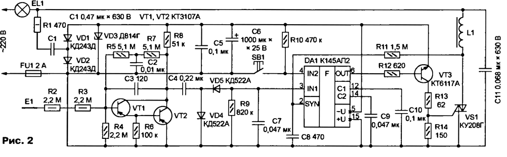
A. BUTOV from S. CORBA Yaroslavl region offers enhanced edition his touch power control [2] control unit on the chip CAP, the description of which can be found in [3]. Unlike the prototype of the new the controller can be enabled to break any of the wires of the network, which is important if they replace the conventional contact switch of illumination
Diagram of the device shown in Fig. 2. The control algorithm is the same: short-term a finger sensor E1 enables or disables the lamp EL1, and when long touch the brightness changes cyclically minimal, to maximum and back in about 5 seconds), the Controller remembers its the status lamp is always switched on installed before shutdown brightness As before, the regulator can be controlled not only by touching sensor, but clicking the button SB1, which operates in a similar way.
(click to enlarge)
The controller being noncritical to the phasing network of wires has been achieved by the introduction of amplifier sensor signal E1 on a composite transistor VT1, VT2. Rectified diodes VD4. VD5 voltage reaching when touched by hand with a sensor -5 to -9 V, now it is enough to control the chip DA1 anyway. The capacitor C2, eliminating OOS DC voltage, increases the rate amplification of the cascade. The capacitor C3 is designed to suppress high-frequency interference.
The node power controller consists of the quenching capacitor C1 with restrictive resistor R1, rectifier (diodes VD1, VD2), voltage stabilizer {the Zener diode VD3) and the filter capacitors C5, C6. The resistor R1 preferably set P1-7 or similar imported discontinuous Remaining constant the resistors of the regulator - S1-4, S2-23 MLT corresponding capacity of the Oxide capacitor C6 is used small. company Rubycon, capacitors CI, C11 - K73-17, K73-24V or K73-50 at a voltage below 400 V or imported, designed for AC circuits, for example, CPF 250V x2. The remaining capacitors - ceramic or film K10-17, km-5, K73-17V. Capacitors K10-7 undesirable because of their low reliability.
Diodes KDA (VD4, VD5) can be replaced by CD, KD521, CD with any letter index 1N4148 or import. Diodes CDD (VD1 VD2) is replaced by KDE-KD243ZH, KD105B-CDP KDE-KDW, 1 n4004 cameras-1 N4007, Zener DG (VD3) - XI, XA, 1N6001B, 1 N4741 A. the VT3 Transistor can serve CTA, CTB, CT, SS8050, SS9013, 2SC1009, 2SC2331, 2SD1616 with any alphabetic index of Transistors VT1 and VT2 can be any of series CT, CT, SS9015, 2SA733, 2SA910, 2SA992
Triac COG (VS1) can be replaced by TS-10, TS-16, TS-class 10 the voltage is not below 4 or imported MAS, MAS. The triac is mounted on U-shaped heatsink dimensions 110 25 mm aluminum sheet with a thickness of 1.5…2 mm permissible load power of the regulator is 350 watts.
The inductor L1 contains 135 turns of wire sew-2 0.51 mm or wound on a ring the yoke CHH ferrite MNS. Before winding the rib ring blunt and wrapped it with a layer of film made of insulating material. Ready the winding is impregnated with insulating varnish. The resistance of the inductor DC approximately 0.3 Ohms. Instead of a ring it is permissible to use a piece of ferrite core with permeability of 400 diameter 8 to 10 mm and a length of 60 mm.
Minimum lamp power EL1 - 25 watts. Completely off the lamp less power will fail due to heat its filament current flowing through the capacitor C1
The cascade transistors VT1, VT2 should be placed as far away from triac VS1 and inductor L1. If the sensor E1 is connected to the controller wire length more than 50 mm, the latter should also be screened. To reduce the interference the sensor triac VS1 preferably electrically isolated from the heatsink.
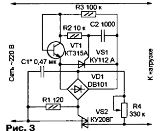
Another design A. BUTOVA - triac phase controller with reduced the level of interference. In most known designs at maximum power load the triac doesn't open until the voltage across it reaches 30…80 V. This leads not only to the "shortage" load of about 4 % power, but to a significant increase in the level generated in this mode of interference. If to get the triac to open when possible lower voltage, these deficiencies will be eliminated or weakened.
In the regulator, assembled according to the scheme shown in Fig. 3, the elements VT1, VS1, R2, R3, C2 assembled analogue dynistor, enabled via a diode bridge VD1 in the chain the control electrode of the triac VS2. As soon as the voltage applied to the emitter junction of transistor VT1, working in our case like the Zener diode exceeds approximately 8… 10 V, reversible avalanche the breakdown of this area and SCR VS1 will be opened. Current pulse discharge capacitor 1 will open the triac VS2. Supplied to the load to regulate power, changing variable resistor R4 time constant of the charging capacitor .
Details of the regulator can be mounted on the printed circuit Board shown in Fig. 4. Variable resistor R4 - SP-1, GPA-ZOA, SDR-35 or SDR-33. On its axis be sure to put the handle of insulating material. Fixed resistors - MLT, S2-23 S2-OPA, C1-4. Capacitor C1 - K73-50, K73-24V, K73-17. K73-16; C2 - K10-17, km-6. Diode bridge - any of the series DB101-DB107 [4], CC, CC. Can to make a bridge and four discrete diodes series CD, CD, CD, CD, 1 N4001 - 1 N4007. Triac COG can be replaced by another medium power, for example, TS-10, TS-16, TS-10, TS-25. Preferably the fourth and higher voltage groups.
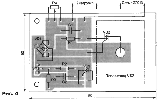
Experience has shown that no matter how low the load, the triac VS2 the necessary heat. Due to a large unmanaged reverse current triac, which is enough for its self-heating and subsequent arbitrary opening. When choosing the size and shape of the heat sink should strive to its temperature in continuous operation at maximum capacity is not exceed 60 °C. heat sink for the triac VS2 motherboard provides.
The establishment of the regulator is reduced to the selection of the capacitor C1 such capacity to when you move the cursor of the resistor R4 from one extreme position to the other was covered all the necessary interval supplied to the load power.
Any triac controller creates interference, so it should be well screened and connected to the network and the load through the filter. Such, for example, as in Fig. 3 in the S. you can "Triac controller increased power" ("Radio" 2000, No. 7, 41).
Literature