


")

The paper proposed a simple active filters, performed on source the repeaters. Low distortion and low order characteristic of such filters, contribute to the achievement of the purity of the sound spectrum-saturated musical signals. This allows them to compete successfully with active filters at the shelter.
The advantages of audio nodes in field-effect transistors can be attributed low harmonic and intermodulation distortion in them the amplified signals. Due to This fact, designers are increasingly used these transistors in the output stages of USC. However, in preliminary cascades such devices are used rarely, mostly in Amateur development. And in vain! Their application allows you to create a simple diagram of the device without total feedback, create a warm "tube" sound. Harmonic distortion amplifiers even with local negative feedback does not exceed 0,1…0,3 %, high harmonics order virtually absent.
The advantages of field-effect transistors especially evident in simple designs. However, in this case, it becomes noticeable their main disadvantage - pretty big technological scatter of their own settings. Due this usually requires customization of each product. It is not obstacle for radio Amateurs, but for mass production of devices with the simplest circuitry of little use. However, and this fact can to consider: is used in small-scale production debugged design transistors from the same batch; within one pack variation options not so great.
The main condition that was posed during the development of the proposed filters high linearity for signals with levels up to hundreds of millivolts in a wide band frequencies at extreme simplicity of the device. If you use p-channel transistors with a cutoff voltage below -3 IN (KSSG, CPSES), the desired mode work on single supply is achieved without displacement of the gate. The coupling capacitor at the input of the cascade in this case is not required. And this further enhances the sound quality.
To calculate the modes of the cascade (Fig. 1) DC and the transmission coefficient it is possible by the method of linear approximation [1]. This method is much simpler and clearer given in [2], provides almost the same results.
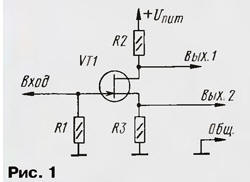
To calculate the slope characteristics of the transistor S, and it is advisable to not use reference and real value. However direct measurement of the steepness in Amateur conditions is difficult. Linear the approximation allows the use to define the structure more convenient for measurement parameters: the initial drain current SNAC and cutoff voltage Uотс. The slope in this case is determined according to the formula:
S= IC nach/Uотс.
The resistance of the resistor in the circuit of the source Ri is possible to choose from the ratio Ri = (3…6)/S. the Output voltage of the cascade runoff can VT1 be estimated from the ratio Uвых = UBXSRC/(1+SRи), and the voltage the signal at the source - by the formula Uвых = UBXSRи/(1+SRи), where S is the steepness transistor; Ri, RC - resistance in the circuit the source and drain (Fig. 1 - R3 and R2 respectively).
The simplest design is a second order HPF on the basis of the source follower (Fig. 2). The disadvantages of this filter is connected with its low transmission coefficient. This parameter depends on the steepness characteristics for common and low-power field-effect transistors with S = 3…7 mA/V will be…0,85 0,8. So calculated (for a single transfer coefficient) values castorocauda elements have to adjust or be used for the calculation of the formula, taking into account the actual ratio of the transmission [3].
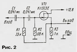
So, when indicated in the diagram the values of parts of the calculated cutoff frequency is 72 Hz, and the real - 85…90 Hz. Although the ratio of the values of R2/R1 - 2 corresponds to the Butterworth filter, cutoff frequency is somewhat higher calculated, and the inflection frequency response is smoother. To increase the steepness of the frequency response in the field inflection, the resistance R1 should be reduced so that the ratio R2/R1 amounted 3…10. The cutoff frequency can be shifted by proportionally adjusting the resistance resistors R1, R2 and the capacitance of the capacitors C1, C2.
The signal at the output of the filter is attenuated by 2…2.5 dB, while reloading the ability of a cascade of low. In these conditions, the maximum undistorted the output voltage will not exceed 500 mV. To overcome these disadvantages can use the combined cascade structure "common origin - a common collector" (Fig. 3), but the signal at the output of this filter will be inverted.
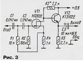
The use of emitter follower at the output of the filter has reduced output resistance is approximately 50 Ohms and improved load capacity. When specified on the circuit component values, the cutoff frequency of about 80 Hz. Gain (2…3 dB) depends on the characteristics of the applied field transistor and the resistance of the resistor R3. The establishment is reduced to the selection of such its value to the voltage at the emitter of the transistor VT2 is approximately was equal to half the supply voltage. In the presence of the oscilloscope exact value resistance is best to choose the symmetry restrictions of the output signal. In the calculation of the cutoff frequency and filter type fair given earlier considerations. For modeling filters are convenient to use program Microcap.
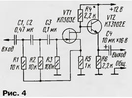
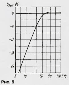
To further increase the steepness of the frequency response, you can apply a two-link chain reverse connection. In Fig. 4 shows a diagram of a band-stop filter for subsonic frequencies with Fcp= 25 Hz, and in Fig. 5 - its frequency response.
Based on the patterns you can make and bandpass filter, required when creating a multiband amplification systems. Diagram of the filter shown in Fig. 6.
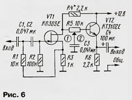
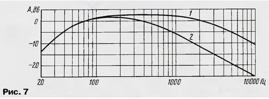
Between the stages are switched tunable passive LPF the first order R5C3. Such a simplified design of filter made possible because the frequency response of the low-frequency dynamic heads in the upper frequencies already has the recession and in most cases can only agree with him the streak the bandwidth of the amplifier. The frequency response of the filter in the extreme positions of the regulator is shown in Fig. 7.
The establishment of a filter similar to those already discussed in the article options filters. It should be borne in mind that the upper limit of the tuning bandwidth is determined by the output resistance of the cascade FET, and it, in turn, the resistance of the resistor R4.
An example of joint use of the described filters is shown in Fig. 8. This unit the formation of bands of LF / MF-HF left and right stereo channels, and sum (mono) signal to the subwoofer. Splitting lanes MF and HF is passive filters at the output of the amplifier. Scheme channel filters identical to the previously reviewed, so we will focus only on the filter, releasing the low-frequency signal for the subwoofer.
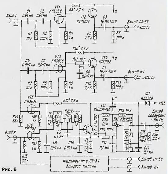
The first stage - adder on two field-effect transistors with a common load R18 similar to that described in [4]. Basic filtering maintains an active LPF the second order made on the emitter follower VT7. The cutoff frequency can rebuild from 40 to 160 Hz dual variable resistor (R20.1, R20.2). Capacitor C8 in conjunction with the output impedance of the first stage forms link of the first order LPF with a cutoff frequency of about 180 Hz. It's almost not affect the course of ripple in the passband, but improves the out-of-band suppression components.
Depending on the location of the subwoofer relative to the speakers of the left and right channels and listener, the phase shift of the signals at the listening position can to distort the sound (the effect of "blurring" or "lag" bass). For correction of phase shift in the subwoofer channel regulator introduced with OS DA1. In the circuit the installed power diode-capacitor filter VD1C11.
This design is specially designed for car audio. The fact that a rather considerable resonance of the cabin, which is manifested in characteristic "the buzz" on bass sounds, picky distresses audiophiles on wheels. The frequency response measurements show at frequencies of 120… 160 Hz "hump" in the amount of from 3 to 8 dB! For frequency response correction in this case it is convenient to use instead of EQ the notch filter. The scheme of such active filter for one channel is shown in Fig. 9 [5].
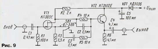
The first cascade amplifier with a split load. Its task is to create anti-phase voltage supply of filter element C2C3R4R5. In law diagram the position of a key switch SA1 is formed facing the bridge with Wine attenuation of about 3 dB. In the left position of the switch on the filter do anti-phase voltage and attenuation on frequency is increased to 5…6 dB. The exact value of the attenuation depends on the steepness of the transistor and the ratio resistors R2 and R3. If equal, the attenuation will be maximum (up to 8 dB), but the output signal will be attenuated relative to the input HB 3…4 dB. The diagram shows the optimal values.
Since the input impedance of the device is very high, to set the filter better near the source of the signal to avoid interference input. Output filter resistance is about 50 Ohms, which is much less than the same parameter most head units. This will allow to exclude the effect of capacity connecting cable, so that the filter simultaneously performs the function of matching device. The enclosure should be metal, otherwise you have to provide it within a screen of copper foil and connect it to GND.
The frequency response of the filter (see Fig. 9) shown in Fig. 10.
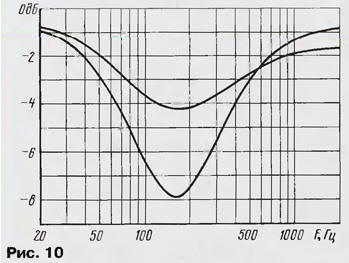
As you can see, it is not just filter, and a real "equalizer environment" (equalizer ambience). Device the same name and very similar frequency response used in top-end models of amplifiers Mcintosh, only the circuitry there is a little more complicated…
In addition to these schemes on devices, you can apply the transistors KSSV-KSZG, KT3102 (with any letter index) or other structures of the n-p-n h21e > 50. In the phase switch you can use any OS, adjusted. for a single gain. Oxide capacitors should be on the operating voltage of not lower than 16 V. The selection of other parts is not critical.
Literature
Author: A. Chechetov, Moscow