


")

Common schemes of crystal oscillators provide phase noise is not worse than -155 dB/Hz relative to the carrier level (the power). Multiplication to 245 GHz worsen this option in the output signal to -87 dB/Hz. When using NBFM, for example, the noise level in the band 16 kHz would be (-87+42) dB, i.e. only 45 dB below the carrier. Thus the dynamic range of the receiver will be only 45 dB, and in the mode of transmission of radiated broadband noise will be 45 dB below the level of the main signal.
In section "Stability improvements" shows that quartz crystals have a temperature instability of ±10 ppm (10-5) 0°C to +70°C. This corresponds to ±100 kHz 10 GHz, when multiplied 100-MHz signal. Temperature compensation can be achieved instability is not worse than 0.3 ppm (3*10-7) or ±3 kHz to 10 GHz, or ±7 kHz to 24 GHz, or ±75 kHz to 250 GHz. To ensure "stone" instability of the local oscillator will help the PLL reference oscillator corresponding to a rubidium frequency standard.
These generators were used in legacy radio navigation devices and you can find them in American stores of illiquid assets. They have temperature instability ±10-9 or 0.001 ppm and allowed the author to achieve long-term instability of ±250 Hz after multiplying on the Amateur range is 241 to 250 GHz. In section "Reducing phase noise" on the example of a traditional crystal oscillator Butler bipolar transistor is shown (Fig.1) that the noise level in the output signal is influenced mainly by the noise of the input transistor to which is applied the signal from the quartz resonator and markedly reduced after increasing the resistance of the entrance.
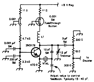
Fig.1
For the circuit in Fig.45 noise level -155 dB/Hz, and after replacing the bipolar 2N5179 the field transistor J310 common-gate, the author received phase noise -172 dB/ Hz. In section "Schema MODES" is a diagram of a voltage controlled oscillator (Fig.2) is the primary node of a low noise crystal oscillator with PLL (low-noise phase-locked crystal oscillator - LNPLXO) developed by the author.
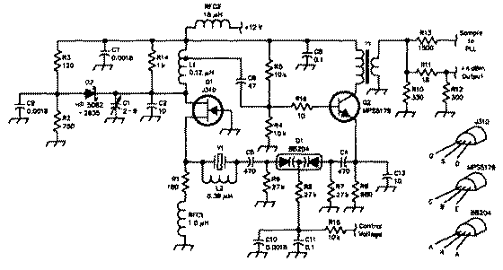
Fig.2
Amplifying the cascade of common-gate on Q1 provides a high impedance input for signal from the quartz resonator Y1 and the emitter follower Q2 - low output impedance of the MODES and, consequently, a low resistance circuit of the resonator. Y1 is excited at the fifth harmonic series resonance, is at-cut, and C0=30 pF, R0<60 Ohms. Contour L1C1C2 selects the desired harmonic. R14 bypasses it to improve linearity and installs the necessary coefficient of chain transfer PIC generator. Chain D2C9R2R3 limits the amplitude of undistorted output. At the point of connection R2R3 set to 1.6 V. When the peak value of the RF signal at the drain of Q1 reaches -2, D2 opens and restricts the further growth of the amplitude of the output signal without changing the operating point of Q1, which positively affects the linearity and noise characteristics of the oscillator. With R2, you can select the output level so that Y1 dissipate no more than 1 mW. To ensure minimal effect of loading on the VCO output signal is taken from the collector of Q2 through the transformer T1 9:1. The PLL for LNPLXO (Fig.3) made according to the standard scheme.
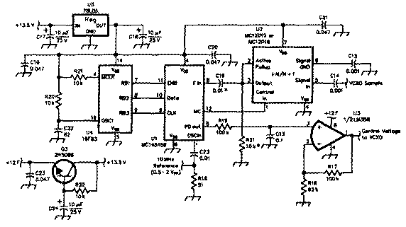
Fig.3
Its basis U1 (MS), comprising a frequency divider R signal high-stability rubidium reference oscillator(input 1/U1); DPKD for pre-divided chip U2 on 20/21 (MS) or 32/33 (MS), frequency VCO (input 8/U1); the phase detector output 5/U1. The signal from the phase detector is fed to the LPF R19C13 whose parameters do not correspond to the recommendations by Motorola and were chosen experimentally taking into account the high quality factor of quartz in the MODES (Fig.46). The system PLL controlled by the microcontroller PIC16F83 (U4), a control program for which (file STEP1199.ZIP) can be downloaded at http:// www.arrl.org/files/qex/. For VHF / UHF transverter on 24,192 GHz, the author uses the mixer on a counter-parallel diodes, wherein geradin must operate at half the frequency equal 11,448 GHz if FC 1296 MHz. To signal LNPLXO (Fig.46, 47) frequency 95,4 MHz to get 11,448 GHz, the required multiplier 120. This is solved by the sequential multiplication of 2, 3,4 and 5.
Author: John Steffensen (KD6OZH); Publication: N. Bolshakov, rf.atnn.ru