


")

The complexity of the design of this receiver compared to popular hams simple synchronous УSW FM receivers, according to the author, justified by the improvement of the main characteristics: the sensitivity and stability work.
The receiver described here УSW FM signals for range 65,8…73 MHz. different from previously published greater sensitivity and the absence of such inherent characteristic disadvantages like instability and settings spontaneous rearrangement to a stronger signal of the neighboring channel. The sensitivity of a synchronous heterodyne receivers is limited by the fact. what "drift of zero" of the DC amplifier affects the host frequency control lo and causes instability of the settings of the receiver. In developed the author of the design is reduced due to the fact that instead of amps constant voltage amplifiers are used alternating voltage, achieved the decrease in "zero drift", which allowed to increase the sensitivity of the receiver, which now is about 8 mV. In addition, the voltage change on the node control the frequency of the local oscillator is reduced by the amplitude limiter ZL1 therefore, under the action of the control voltage the frequency of the local oscillator will not be to change by more than 100 kHz. This prevents spontaneous setting on a nearby frequency radio station.
The receiver consumes about 34 mA. Its structural scheme is depicted in Fig. 1.
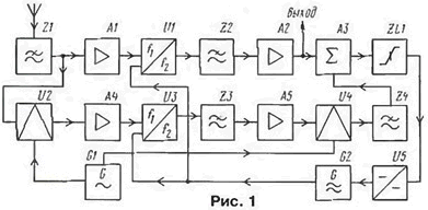
The received signal from the antenna via two-tier low-pass filter Z1 and the high-frequency amplifier A1 is fed to the signal inputs of the mixer U1. On the other input voltage of the local oscillator G2. If the signal frequency, and lo not equal, then ia the mixer output AC voltage is formed the beating, which, through the low pass filter Z2, the low frequency amplifier A2. the adder A3 and amplitude limiter ZL1 is supplied to the node control frequency lo U5 and changes the frequency of the local oscillator G2 such that instant the difference frequency signal and the local oscillator is reduced to about 72 Hz. This value the frequency is determined by the lower boundary of the bandwidth of the amplifier at low frequencies A2.
The signal output from the LPF Z1 was also fed to the signal inputs of the modulator U2, the second input of which receives an alternating voltage of rectangular shape a frequency of 20 kHz from the auxiliary generator low frequency G1.
As a result, the output of the modulator is formed modulated in amplitude high-frequency voltage through high-frequency amplifier A4 is fed at the signal inputs of the mixer U3 (fc), to the second input of which receives the voltage from the oscillator G2 (fg). At the mixer output variable appears voltage with frequency of 20 kHz. modulated by amplitude fluctuations of the differential frequency (i.e., the beat frequency fb = fc - fg). which through a low pass filter Z3. the low frequency amplifier A5 is supplied to the signal input of the demodulator U4.
To the second input of the demodulator is fed an alternating voltage with a frequency of 20 kHz generator G2. At the output of the demodulator is formed of alternating voltage, frequency equal to the instantaneous frequency difference signal and the local oscillator, then through it two-tier low-pass filter Z4. the adder A3 and amplitude limiter ZL1 is supplied to the control node of the frequency of the local oscillator U5 and changes the frequency lo G2 so that the PLL of the receiver switches from the mode beating on hold. The difference frequency signal and the local oscillator, wherein there is a transition on hold, is determined by the cutoff frequency of the filter and Z2 is 10.6 kHz (minimum signal).
Thus, when the PLL into hold mode (synchronization) quick treatments frequency of 72 Hz < f < 10,6 kHz) are compensated by the channel, comprising from the low-pass filter Z1, the high-frequency amplifier A1, mixer U1, lowpass filter Z2. the low frequency amplifier A2, the adder A3, the amplitude limiter ZL1 node control frequency of U5 and the local oscillator G2.
Slow goings frequency (< 330 Hz) are compensated by the channel, consisting of modulator U2, the high-frequency amplifier A4, mixer U3, lowpass filter Z3. the low frequency amplifier A5, the demodulator U4, lowpass filter and Z4 generator G1. The AC voltage of the audio spectrum (72 Hz < fz < 10.6 kHz), proportional to the deviation of the instantaneous frequency of the signal at the input receiver, amplifier with low CASL A2 arrives at the receiver output.
The dynamic characteristics of the PLL are determined by the amplitude of the input signal form and frequency response of a lowpass Z2. which is a simple RC circuit. The shape of the open-loop frequency response of PLL similar to the shape of the frequency response link of the first order, so the PLL operates in synchronization with a sufficiently large amplitude range of the input signal. The receiver doesn't have the AGC system, so with a very large amplitude of the input signal of the PLL snowspeeders (quasiconcavity). But in this case, the receiver stores performance, since the excitation of the system PLL is not reflected in the quality of the output signal (frequency of self-oscillations in the system PLL is above 50 kHz).
Receiver selectivity adjacent channel is determined by the parameters of the LPF Z2, and the selectivity of parasitic channels of reception (on the harmonics of the local oscillator (lo) - parameters of low-pass filter Z1.
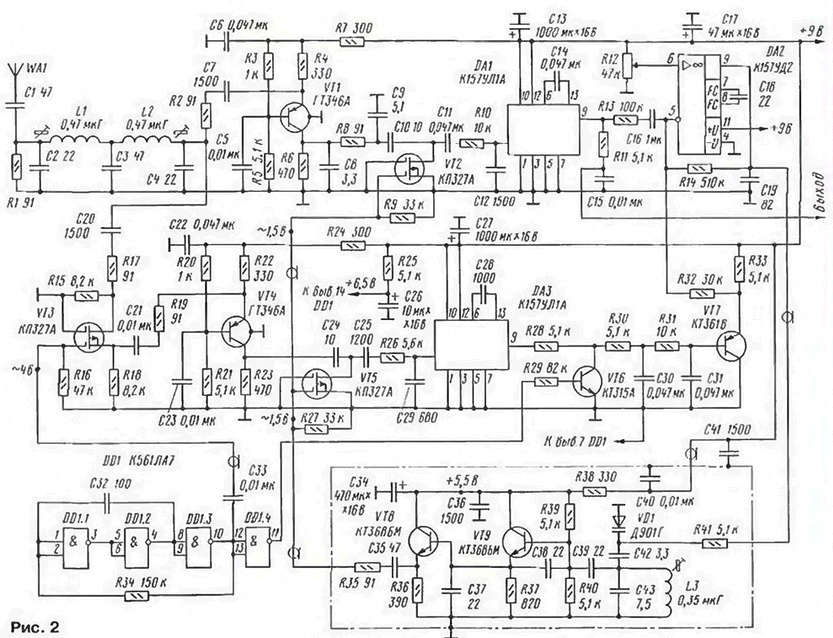
Schematic diagram of the receiver shown in Fig. 2.
(click to enlarge)
The signal from the antenna through the coupling capacitor C1 and the LPF. formed by capacitors C2 - C4, and coils L1.12. arrives at the HRC performed on the transistor VT1. This the amplifier serves to reduce the penetration of the oscillations of the local oscillator in the input chain, increased its small at Ku < 5. A transistor connected in the circuit with a common base that provides high linearity and UHF promotes the noise immunity of the receiver (on a similar scheme implemented and UHF transistor VT4). The characteristic impedance of the filter Z1 close to 75 Ohms. and its frequency the cutoff is 75 MHz.
Elements R6. C8. R8. C9 form a phase shifter which shifts the phase high-frequency voltage supplied to the mixer made the transistor VT2. for a few tens of degrees. It is necessary for improving the sensitivity of the receiver. The thing is. what is in hold mode (synchronization) the phase shift oscillation signal and the local oscillator input at the mixer VT5. close to 90. At the same time due to the delay of high frequency signal in the modulator VT3 phase shift between the oscillation signal and the local oscillator inputs mixer VT2 may be different from 90°. When receiving weak frequency modulated signal with a large frequency deviation, this can lead to short-term disruptions synchronization in the moments of the maximum deviation frequency. The circuit, consisting of element R6. C8. R8. S9. provides additional high frequency delay signal that allows you to set the inputs of the mixer VT2 phase shift hesitation about 90°.
Construction of low-pass filters, Z2 and Z3 (respectively on the elements R10. C12 and R26. S) amplifiers and low frequencies A2 and A5 (on chips DA1 and DA3) both channels the same and differs only in the values of the elements used. The low-frequency signal is taken from the output of DA1. elements R11, C15 are used to correction of high-frequency pre-emphasis.
The function of the adder A3 and amplitude limiter ZL1 performs a chip of DA2. Modulator U2 performed on the transistor VT3, and the demodulator U4 - transistor VT6. The role of the lowpass filter Z4 do the elements R30, C30. R31. C31. Emitter the follower transistor VT7 reduces the influence of the adder on the filter parameters lower frequencies. The node control frequency U5 performed on the varicap VD1, heterodyne G2 - transistors VT8, VT9. and auxiliary low-frequency oscillator G1 - on DD1 chip.
The steepness of the site frequency control Sγпр - 35 kHz/V. therefore, when the frequency deviation (f = 50 kHz) audio frequency voltage across the capacitor C19 is about 1.5 V, and the output of the receiver (C15) is about 0.3 V.
Configuring the receiver to the radio frequency produced by varying the inductance coil of the oscillator L3.
The receiver is assembled in the case of duralumin sheet. In its manufacture used point wiring. The local oscillator is enclosed in a screen, in addition, is connected with capacitors C19 (chain management), C41 (power) and with the gates of transistors VT2 and VT5 (lo signal) segments of the TV coaxial cable. On case shielded wire connecting pin 10 DD1 shutter transistor VT3, but not necessarily.
The device can be used fixed resistors MLT-0,125, capacitors - ceramic, for example. CT or km. Capacitors C2 - C4, C37 - C39, S, S should have low TKE. Oxide capacitors may be of any type.
As transistors VT1, VT4, VT8 and VT9, unless recommended by the diagram, you can use other microwave related system and with a cutoff frequency of 900 MHz, the capacitances of the junctions are not more than 2 pF and low the time constant circuit of the OS (no more than 10… 15 PS). For transistors VT1 and VT4 especially the importance of the time constant circuit OS and the noise factor. In case the need to replace them suitable KT368, CT, CT, CT, CT alpha indices corresponding to the parameters mentioned above. As VT6 and VT7 you can use any high frequency corresponding structure: CT. KT3102. CT with any alphabetic indices, etc., Instead KOA (DA1 and DA3) you can use COB, COD (DA2) it will replace any of the operations the amplifier is of General application, the method is limited to work when specified in the scheme supply voltage. As VT2, VT3, VT5 suitable CP with other letter indices.
Coils L1 - L3 are wound on the frame with an outer diameter of 6 mm wire PEL-1 0.45 mm and contain five turns. Their inductance is adjustable brass the podstroechnik and threaded M5.
With proper installation and proper radio setup receiver extremely simple. You need a variable resistor R12 is set on the capacitor C19 a voltage of +4.5 V. then, rotating podstroechnik coil L3. to configure the receiver on the radio, achieving the best sound quality. In the presence of interference you may need to precisely adjust the border of the LPF trimmers coils L1 and L2. To reduce the mutual induction these coils should be placed so. to the axis were perpendicular.
The parameters of the receiver can be improved. For example, to increase the parasitic suppression reception channels on the harmonics of the local oscillator, using the input three-tier LPF. But in this case the coil of the filter it is desirable to screen.
By reducing the resistance of the resistor R13 is possible to increase the width of the strip capture on audio frequencies and thus about two times increase the receiver sensitivity. But it requires a greater precision in setting lo. Unfortunately, this worsens the signal-to-noise ratio at the output receiver. Have to choose that in the specific conditions of acceptance are more important.
Author: A. Sergeev, Sasovo, Ryazan region