


")

In Amateur radio shortwave equipment widely used balanced modulators based on semiconductor diodes, built by the loop scheme. They provide a deep suppression of the signals have a wide frequency range.
However, the SSB signal filter way these virtues are not used. Indeed, there is no need to suppress low frequency modulating signal as the modulator is always followed by a narrowband filter. There is no need the high bandwidth of the modulator.
On the other hand, the use of a diode ring balanced modulator leads to unnecessary complication of the circuit. The fact that both inputs of the modulator nishani, so you have to apply a cathode or emitter follower. In addition, to avoid nonlinear distortion in diode modulators cannot give the signal, the value of which exceeds 100 - 150 mV. Given the loss in the diodes and balancing resistors, one should not expect that the magnitude of the output signal exceeds 10-15 mV. Therefore, after the modulator need additional amplification cascade.
The figure shows a diagram of a balanced modulator on the varactors used in the lamp-transistor transceiver (see "Radio", 1974, No. 8) and showed good results.
Capacitance serially connected varactors together with the inductance of the primary winding of the transformer TR1 forms a resonant circuit. The condenser NW serves to tune it into resonance with the input high-frequency signal. Resistor R5 regulate the bias voltage applied to the varactors.
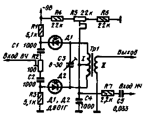
With equal stress on both varactors their capacity will be equal. Then the RF currents flowing through the primary winding of the transformer cancel each other out, and the transformer secondary voltage is missing. For final balancing modulator is designed resistor R2.
Upon receipt of the input LF signal is an imbalance. With its positive half wave capacity VA-recap of A1 increases, A2 decreases. With negative half wave the capacitance of the varactors are changed in reverse order. Accordingly vary and magnitude of high-frequency currents in the act of modulating the LF signal and the secondary winding of the transformer appears modulated RF signal with a suppressed carrier.
The suppressed carrier is very deep. Within one and a half years of operation of the transceiver it remained in the range of 50 dB.
Both inputs of the modulator high resistance, so the emitter followers is not required. When the RF signal by a value of 1 V and the low frequency signal magnitude 2.5 V output signal amplitude of 350 mV at load impedance 600 Ohms. Nonlinear distortion is not noticeable.
Transformer TR1 is wound on a ferrite ring core VC-2 CHH,2. If the modulator is designed for a frequency of 5.5 MHz, the primary winding must contain 38 turns of wire sew-2 0,16 with a branch of the middle. The secondary winding contains 9 turns of the same wire. If the load modulator high resistance (junction field-effect transistor or tube), the number of turns of the secondary winding should be increased.
The modulator may be applied to the varactors D, D and SW102 with any letter index.
Author: V. Galneryus (UP2NV), Kaunas; Publication: N. Bolshakov, rf.atnn.ru