


")

To obtain the amplitude-modulated oscillations with a suppressed carrier in communications technology typically use balanced diode ring modulators. They work well on relatively low frequencies, but at frequencies above 10 MHz such modulators deteriorates the accuracy of balancing and accordingly the suppressed carrier. This is due to the difficulty of identifying diodes with identical characteristics and growing at the RF shunt harmful effect of the capacitances of the diodes.
The proposed balanced modulator (Copyright certificate № 627560. Bulletin No. 34 of 5.10.78) largely devoid of this shortcoming. It is T-shaped bridge circuit (Fig.1). Actually the T-bridge contains a symmetrical high-frequency transformer T1 and two resistances Z1 and Z2. They can be both active and reactive (inductive or capacitive). The transmission coefficient (the ratio of the output voltage Uвых to the voltage developed by the generator carrier G1) T-bridge is equal to zero under the condition Z1= =4Z2. If the impedance Z2 to increase. the output of the bridge there is a voltage in phase with the generator voltage, as will be dominated by the current in the longitudinal branch of the bridge containing Z1. If the impedance Z2 to reduce, we will prevail, the current through the left (the scheme) half winding of the transformer T1 and the transverse branch - impedance Z2. The output in this case there will be a voltage induced in the right half of the winding, and anti-phase voltage of the generator. Thus changing in time with the frequency of the sound resistance of one arm of the bridge, you can get a DSB signal.
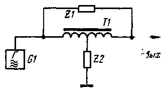
Fig.1
The practical scheme of the modulator operating at a carrier frequency of 28 MHz, is shown in Fig. 2. The longitudinal resistance of the 7.1 branch is capacitive
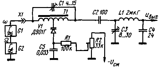
Fig.2
the resistance of the capacitor C1, and the cross-Z2 - capacitance VA-recap V1. The voltage is fed to the mixing with varicap tuning resistor R2, which are balanced modulator. If the source offset from the common wire is connected to the negative terminal, then you should change the inclusion of the varicap on the opposite. The capacitance of the capacitor With the/ needs to be four times less than the capacitance of the variable capacitor to a given voltage mixing. When the varicap effect of the audio modulating voltage. its capacity varies and T-bridge razbalansirovat in one way or another, providing amplitude modulation with suppressed carrier.
Voltage carrier and audio frequencies fed to the modulator (the generators G1 and G2. in principle, can be included in both series and parallel). In this case the input impedance for audio frequencies becomes very large and reaches tens of megohms. Because of this modulator can be connected to any high impedance source bass signal G2, for example the RC phase shifter (in the design phase SSB exciter). The modulating voltage can be summed in a different way: the top of the lead of the capacitor C5, reducing its capacity to 1000…3000 PF to avoid blockage of the higher audio frequencies. The input impedance will then be equal to the resistance of the resistor chain R1 mixing. The slider of the variable resistor R2 should be connected to GND through capacitor 0.1…10 µf Input impedance of the modulator for carrier frequency generator G/ is much smaller. it is capacitive in nature and is approximately 200 Ohms.
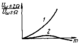
Fig.3
The coupling capacitor C2 prevents the audio voltage at the output of the modulator. For approval of the modulator to the load is P-loop LIC3C4, tuned to a frequency signal. When the values of capacitors, shown in Fig. 2, the modulator is in good agreement with high-impedance loads (gain stage executed on a tube or a field-effect transistor). To align with the low-impedance load, you should use a capacitor C4 with a larger capacity, achieving maximum impact power modulated signal. P-loop provides good filtering of harmonics of the carrier frequencies 2f, 3f, etc. Adjusting this circuit, you can achieve good linearity of the modulator.
Nonlinear distortion during the operation of the modulator active on the load manifest: the amplitude of the output signal during a negative half-wave modulating voltage (when the capacitance of the variable capacitor increases) slightly more than positive. This is equivalent to the appearance of the second harmonic of the modulating signal. The distortion is due to the reduction of the internal capacitance of the modulator increases the capacitance of the varicap. Growth factor modulation of t harmonic distortion significantly increased (curve 1 in Fig. 3). The corresponding waveform of the output signal shown in Fig. 4,and.
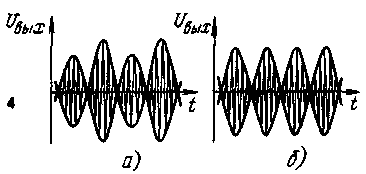
Fig.4
Describes the distortion is almost completely eliminated with a small detuning of the output circuit up the frequency. when the impedance becomes inductive. With further detuning appear similar distortion (but reduced for the other half wave of the modulated signal). Thus, adjusting the capacitor circuit NW, it is possible to achieve very low harmonic distortion (curve 2 in Fig. 3 and the waveform in Fig. 4, b). When properly tuned loop, the instantaneous value of harmonic distortion in the worst case (the amplitude of the LF signal such that the modulation depth t corresponds to the maximum of curve 2 in Fig. 3) does not exceed 2…3%. Balancing modulator adjusting circuit is not broken. The modulator can be applied to the varicap of any type with a rated capacity of not less than 30 pF. Transformer T1 is wound on .the ring core (size Khh) of ferrite MN and contains 2x10 turns of wire PELSHO of 0.25. You can use other ferrite ring cores with permeability from 30 to 400. The two halves of the transformer winding is wound simultaneously by two folded wires together. Then the beginning of one of them is connected to the end of another, forming a middle pin. Coil LI has 20 turns of the same wire wound around a cylindrical frame (tube) with a diameter of 6 mm.
Configuring the modulator is simple. Setting the bias voltage on the engine tuning resistor R2 In about 6, roughly balance the modulator capacitor C1 to the low carrier signal at the output. Accurate balancing is achieved by adjustment of the resistor R2. Then, submitting a low-frequency signal, observe by means of high-frequency oscilloscope the output voltage waveform (see Fig. 4) on the capacitor C4 I adjust the output P-loop to the maximum amplitude and minimum distortion. To configure the modulator without oscilloscope, listening to the signal at the corresponding receiver. But in this case, the adjustment elements C1 and R2 is the minimum carrier, and Sz - at the best quality and the volume of the signal.
Experimental verification of the modulator was performed on the carrier frequency is 28 MHz. The amplitude of the voltage of the carrier frequency was 1 V, and the low-frequency signal - 4B. Thus obtained was the amplitude of the output signal 0.35 V in suppressing Nessa at least 30 dB (minimum value that can register are the author of your measuring equipment).
In conclusion, it should be noted that the modulator can be used to obtain not only DSB signal, but ordinary amplitudemodulated, much razbalansirovat his capacitor C1 I. thus, restoring bearing. In this case, you can get very deep AM (almost 100%) with low distortion.
Author: A. Polyakov (RA3AAE), Moscow; Publication: N. Bolshakov, rf.atnn.ru