


")

The modem is designed mainly for the use of the packet radio systems, but can also be used in radio systems for General purpose and wired systems.
The modem does not require a mandatory hardware controller packet communication, works with any software controllers L2, TFPCX, TFX. When using the emulator Kiss-mode TFKISS can use a software TNC programs TCP/IP type KA9Q, TNOS, JNOS. When used in the ISO OSI (Protocol X25/AH) terminal program TRC and program Host-mode
FBB speed double through software compression in 2 times. Similarly, when working according to the standard ARPA (TCP/IP). The structure of the modem includes 3 domestic circuit series 561 and 1401 (CGG, CIR, UB). All 59 items. Functionally, the modem consists of two completed parts parts: receiver and transmitter. Section of the receiver and transmitter operate independently of each other. The total current consumption of all the modem does not exceed 3.2 mA through the circuit +5 V. Analog present modem chips are TSM, FX419, AM. The modem on a chip DM contains two buildings and has 45 items. With almost the same number of elements in both modems undoubted advantage of modem on the domestic element base is the ability to obtain speeds above the nominal value for more wideband voice frequency.
At speeds 2400/2800 Baud proposed frequency the modem is also close to that of a full-duplex FFSK, GMSK, 4-L FSK chip FX469, FX589, FX909, FX919. It has a high sensitivity and high statistics on the frequency of failures, interference conditions. But unlike listed single-chip radio modem requires no connection DC voltage on the varicap of the transmitter and from the output of the frequency detector of the receiver. This limitation is the main obstacle in working with radios that do not have these findings for the modem. In addition, in the modem there is no error propagation, scrambling, as in GMSK modem that does not allow the latter to operate with signals below 8…9 points on the S-meter.
We present frequency modem may have five regulators:
- regulator medium frequency transmitter;
- the controller is the deviation of the transmitter;
- the average frequency regulator receiver;
- the controller is the deviation of the receiver;
- the regulator duty cycle of the received signal and switch lanes reception (2,5/5 kHz).
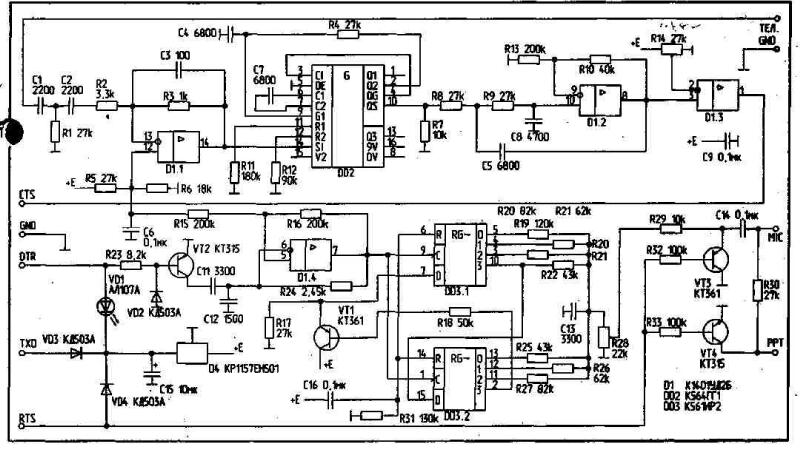
The modem circuit shown in the figure. The receiver is constructed by the PLL. At the entrance there is a zero cross detector circuits D1.1. From the output of the zero cross detector signal is supplied to a frequency detector PLL IC D2. The output signal of the PLL is fed to the low pass filter of the second order on the chip D1.2. At the output of the threshold device on the chip D1.3. Constant of the PLL circuit is determined by the chain R4 C4. Capacitor C7 determines the frequency. The resistance of R11 sets the average frequency, a R12 - frequency deviation.
The receiver requires setting of threshold element by setting the value of the resistance R14 to obtain a duty cycle equal to 2. The transmitter is built based on the FM-modulation continuous phase. Can be the following types of ratios without breaking phase: 0,5/1; 0,75/1,25; 1/1,75; 1/2 periods of subcarrier oscillations.
The resistance R23 and the diode VD2 provide key operation mode control the mode of the transmitter (chip D1.4.), which is the transistor VT2. Resistance R26 and R17 together with the capacitors determine the frequency options.
The resistance R24 and capacitors C11, C12 determine the parameters of the transmitter frequency.
Speed and frequency are given in table.1, where FH is the lower frequency, Fcp - average frequency, FB is the upper frequency.
Table 1
The transmission speed (Baud)
Frequency (Hz)
during manipulation 0/1
FH
Fcp
FB
300
1600
1700
1800
10/12
600
1500
1700
1900
5/6,3
1200
1200
1700
2200
1/1,75
2400
1200
1700
2200
0,5/0,875
4800
2400
3400
4400
0,5/0,875
The table is made in such a way as to ensure minimum switching when switching 1200/ 4800.
At speeds 300/600/1200/2400 Baud modem works in a typical voice channels at a speed of 4800 Baud - non-standard voice channels (double-wide).
VCO transmitter is made on the chip D1.4. Its output signal is supplied to a ring counter. A ring counter performs the functions of forming a stepped sine signal, modulated with the frequency of the continuous phase (16-speed sine wave without breaking phase at the output of the resistive adder). Output signal spectrum, thus obtained, has a minimum width equal to 1.15 and lane deviation. VCO operates at a frequency of 16 times the frequency of deviation, specified in the table, and is controlled by the input digital stream.
On transistors VT3 and VT4 are the elements of the shunting of the output signal and control switching of the transmitter. On elements VD1, VD3, VBW'eor bran diagram parasite power from the RS232 of the computer and on the chip DD4 - stabilizer voltage of 5 V.
Led VD1 (ALA) is an indicator of freezing the RS232 port, the operation of transmission and reception. Readout is performed on the basis of the partial change in the luminosity of the diode. There are the following modes. If the program is unloaded from RAM, and the led lights, then hung port. The total illumination means that the modem is working, and loaded in the RAM resident program TNC. When transmitting the brightness of a luminescence diode VD1 is reduced by 50%, and the reception is at 30%. Changing the settings of the resistances R11, R12, R24 smoothly or discretely using switches, it is easy to obtain the necessary transfer rate in the normal channel tone frequency or channel double-wide. To obtain five speeds these impedances can be performed in the line of three, five resistors mounted on a wall switch or on the Board. It is most convenient to perform a number of these resistances on the basis of resistance 19-1 JV. The inaccurate the nominal frequency of 20% a significant impact on the operation of the circuit of the national Assembly provides.
The decrease in the capacity value of the capacitor C8 twice gives you twice the bandwidth. The design of the modem could be next. The modem runs on bilateral Board width of 75 mm and a length of 78 mm. the Fee is soldered into the ends of the two 25 pin connectors. The housing is U-shaped and covers the height and length of 3 mm connectors. The flat bottom part of the housing is inserted between the thrust flanges of the connectors. The installation of the housing is performed without screws through the bottom latches at the sides of the U-shaped housing. Switches and variable resistances are installed from bottom side of the Board. To access these features, provided the holes in the flat bottom portion of the housing.
RSC "Energia",
head collective radio RZ3DYK,
V. BATUKHTIN (RV3DGA),
Ph. D. S. STREKALOVSKY (RA3DQE),
141070, Kaliningrad,Moscow region.,
Kalinina str., 15, 15.T./f. (095)5133738.
Publication: N. Bolshakov, rf.atnn.ru