


")

In many modern stabilizers to improve their quality indicators used operational amplifiers, having great gain and stable characteristics. However, relatively simple modification of traditional the scheme transistor stabiliser significantly improve its technical characteristics and to avoid some of the difficulties occurs when designing stabilizers with application Shelter (especially in devices with regulation of the output voltage within a wide range). High ratio stabilization described power supply due to amplifier with dynamic load.
Source reference voltage is assembled a field effect transistor that makes it possible to reduce output impedance stabilizer and get deep regulation the output voltage.
Main specifications
Voltage at the entrance of the stabilizer, Volts30
Limits regulation of the output voltage, Volts1 29…
Maximum the load current, Amps2
The coefficient voltage, dB60
Output resistance, mω0,5…10
Temperature the instability of the output the voltage in the interval temperature 20…50* C, more than, %0,5
Instability output voltage the stabilizer is usually consists of instability model voltage and drift op amp. In the described stabilizer it is mainly determined by only temperature drift of the first the active element.
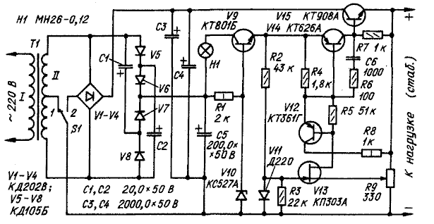
Stabilizer (see diagram) consists of two amplifiers with dynamic load serial control. First collected on transistors V13, V12, where V13 included on the common shutter, and V12 - General collector; the second on transistors V14, V15 V14 - General the emitter and V15 - General collector). The signal return communication with engine resistor R9, applied to the source transistor V13, increases without invert phase, and is supplied to the base of transistor V14. The transistor works in V13 the regime close to the cutoff current. The voltage between the source and shutter is in the exemplary stabilizer. Chain R2R3V11 only serves to temperature compensation change the drain current transistor V13 (without it when confined to a common wire the gate of this transistor the output voltage stabilizer is changed to 3…5% in the temperature interval 20… 50 °C).
With the collector of transistor V14 proinvertirovanny and the amplified signal is transmitted to base strong regulatory transistor V15.
Managing the element is powered by parametric the Zener diode stabilizer V10 and the transistor V9. For more high utilization voltage of the main rectifier (see article "Improving low-power voltage stabilizers" - "Radio", 1981, No. 10, p. 56) V1 - V4 stabilizer transistor V9 powered by a multiplier the voltage on the diodes V5-V8 and the capacitors C1, C2. Multiplier connected to the secondary winding the transformer T1. Lamp H1 serves to limit the collector current through transistors V9, V14 and basic current of the transistor when V15 short circuit in the circuit the load indication the overload. At the moment overload due to increases the base current transistor V15 happens the decrease of the input voltage parametric stabilizer up to level 30 In, where this voltage is almost fully falls on the lamp for H1 less voltage drop transistors V9, V14 and emitter the transition of the transistor V15. Current this circuit does not exceed 120…130 mA, which is less than the maximum valid for its elements.
In the stabilizer used wire AC a resistor with a valid the power dissipation of 3 W (PPB-3, PP3-40). Transistor V13 you need to pick up with small the initial current value drain, then lower the boundary of the output voltage stabilizer will be close to 1 V. the drain Current of the transistor when the voltage between the drain and the source 10 and the stopper, closed on the source, must be within 0.5…0.7 mA. When mounting stabilizer between the diode V11 and the transistor must V13 to ensure good thermal the contact, which is enough glue them to the hull. Transistor V15 is desirable to choose with great static coefficient current transfer base. Except indicated in the diagram, can use a silicon the series transistors CT, CT, CT, CT, CT, CT (V12), CT, CT (V14), transistors KT815, with CT any letter index, CTB (V9),CTA, CTA, with any CT letter index (V15).
In the stabilizer can be applied and germanium transistors MPA, as well as any of the series MP, MP, MP, MP (V12), GT, GT, P-P (V14). Instead KS527A can apply Zener D, DD (two in series), D, DV (three consistently). Transistors V9 and V14 is desirable to set on small radiators (with useful area 20… 30 cm2).
For transistor V15 necessary radiator with useful area at least 1500 cm2. For the purpose facilitate thermal mode this transistor you can see step the voltage change at the input stabilizer switch S1, designed for a current of 2 A. In position 1 on the entrance the stabilizer serves 15 In, and in position 2 - 30 V. When the switch is in position 2 and the load resistance is close to a minimum, stable the voltage should not be set less than 15 V.
Network the transformer is wound on the yoke transformators-60. Primary winding is left without changes secondary rewound; it contains 200 turns (100 turns on each the coil) of PEV-2 1,16.
For improve the reliability the stabilizer can to complement the protective the device described in the article "Protective device for transistors" ("Radio", 1980, No. 9, p. 63). Occasional in the stabilizer high-frequency generation you can suppress or the increase of the nominal value capacitor C6, or switching in the circuit base transistor resistor V15 resistance 5…10 Ohm 1 watt. To ensure stable operation stabilizer installation you need to perform conductors minimum length having a large section the conductors.
Author: A. Grigoriev; Publication: www.cxem.net