


")

Once the author of this article took quite powerful and reliable power source with adjustable in a wide the range of output voltage. After reviewing the available literature, he came to the conclusion that for review devices have disadvantages: linear stabilizers large size (due to the need of the use of the oxide of big capacitors and heat sinks), the PWM stabilizers rather narrow control range and output the voltage present high frequency ripple, and the devices with the improved quality (limited current, readout modes, switching of the transformer windings, etc.) is relatively complex. I had to look for other solutions that and as a result was developed by the power source is free from these disadvantages.
The proposed laboratory power source applied a two-step conversion of the rectified voltage: The PWM conversion to an intermediate voltage and a subsequent linear stabilization. Main technical characteristics device are as follows: the limits of regulation of the output voltage from 1.3 to 30 V, the coefficient of instability in voltage - 0,07 %/In, the instability of the current load of 0.1 %, maximum input (AC) voltage of 27 V, conversion efficiency at maximum load current is not less than 70 %. You can change the threshold current up to 1.2 A, there netrogena the short circuit protection with led indication. The source is characterized by small size, minimal heat loss (at load current to 0.3 And the heat sinks are not required).
Block diagram of the device shown in Fig. 1. Input voltage Uвх transformed PWM Converter DA1 in intermediate Ypres, which, in turn, is input to the analog stabilizer DA2. Feedback through differential amplifier DA3 supports necessary for DA2 voltage drop (for LM317 - 2.5 V), whereby the the heat loss for DA2 minimum.
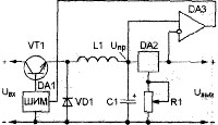
Fig. 1. Block diagram of the power source
Schematic diagram of the power source shown in Fig. 2. Rectified voltage from the output of the bridge VD1 is smoothed the capacitor C1 and applied to the input of the PWM Converter collected on elements DA1, VT2, VD2, L1. The switching circuit DA1 - model reduction [1]. The use of chip CREW have minimized the number of passive elements, but put the maximum input voltage that such inclusion should not exceed 40 V. the PWM with cumulative inductor L1 and the diode VD2 generates an intermediate voltage of Ypres on the capacitor C4.
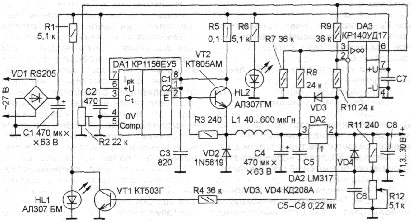
Fig. 2. Schematic diagram of the power source
On integrated circuit stabilizer DA2 assembled linear voltage regulator. Control variable resistor R12. Diodes VD3 and VD4 protect the chip from reverse currents and negative voltages and entered in accordance with the recommendations for its use [2].
Oh DA3 and resistors R7-R10 form a differential amplifier that monitors the voltage drop across the regulator DA2. The gain DA3 is chosen to be equal to 1.5, which allows you to maintain a set value over the whole range of voltages and currents, including for short-circuited output. A trimming resistor R2 regulate voltage drop at forging.
The elements VT1, HL1, R1 made the short-circuited alarm output status. In normal operation, the transistor VT1 is opened so that the voltage drop does not exceed a few tenths of a volt. When the voltage at the output source to 0.7 V or less, the transistor VT1 is closed and HL1 led begins to glow. Engaged state of source power is indicated by an led HL2.
Very interesting is the role of the resistor R5. When the voltage across it is more than 120 mV (mean value, as determined empirically) effective internal pulse-width limiter circuits DA1, turning it into a current source. This property CREW you can use to limit the maximum load current. For example, when the resistance of this resistor, 0.1 Ohm, the source is capable of delivering to the load current up to 1.2 A, and when R5 = 1 Ω only up to 120 mA. By installing a resistor the resistance of 0.5 Ohm and thereby limiting the load current value 240 mA, you can opt out of the heat sink for the chip from DA2 and external current key PWM Converter (excluding the transistor VT2, a resistor R3 and a connecting pin 2 DA1 to a connection point of the inductor L1 and the diode VD2). In this case, the size of the product will be not much bigger than a matchbox.
As the key VT2 can use any transistor with a static current transfer ratio base and more than 30 the allowable current collector is not less than 3 A. the Author used CHAM. He has a good frequency properties, so small switching loss. Very well 'behaves' in this place MOSFET IRF3205 - he doesn't need a heat sink at currents up to 1 A.
The inductance of the inductor L1 can be anywhere from 40 to 600 µh, the only requirement is that it must be designed for the current at least 1.5 A. Resistors MLT, C1-4 with a tolerance of resistance from nominal ±10 %, trimmer resistor R2 - multi-turn wire SP5-VB or similar, R12 AC - any type of resistance 4,7 6,8…com. Capacitors C1 and C4 - oxide C50-35 capacity of 220…470 µf rated voltage 63 V, the remaining ceramic (CH2, K10-7, K10-17, etc.).
The establishment of the power source is to install a trimming resistor R2 of the voltage of 2.5 V between pins 2 and 3 DA2 (at 50% load).
Literature
Author: S. Murali, Dimitrovgrad, Ulyanovsk region; Publication: www.cxem.net