


")

The article describes a simple and inexpensive (according to the author, the value of all components does not exceed one hundred rubles) AC adapter with an output a voltage of 5 V and a load current of up to 4 A.
The power source is a single-ended flyback Converter the voltage excitation. The distinguishing feature of the proposed the device is the lack of specialized chips, simplicity and low cost in the manufacture.
Main technical characteristics
- The maximum output power, W......20
- Output voltage, V.....5
- The maximum load current, And......4
- The interval of the input voltage, ......187 242…
- Input voltage frequency, Hz......50
- The instability of the output voltage, %, not more......2
- The amplitude of the fluctuations, %......1
- The interval of working temperatures, °C......-40…+70
- Dimensions, mm......80x65x20
- The mass of the heatsink, g......120
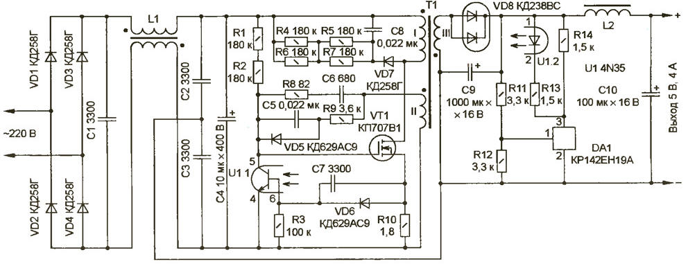
Diagram of the device shown in the figure. The power source comprises a network the rectifier VD1-VD4, noise filter L1C1-C3, a Converter a switching transistor VT1 and pulse transformer T1 output the rectifier VD8 with filter C9C10L2 and site stabilization performed on the stabilizer DA1 and the optocoupler U1.
(click to enlarge)
The device operates as follows. After turning on the power source switching transistor VT1 turns and the primary winding of the pulse transformer T1 current begins to flow. In the feedback winding II transformer induced EMF, which is the chain of positive feedback - resistor R9, diode VD5, the capacitor C5 is supplied to the gate of a field effect transistor VT1. Resulting in the development of avalanche process, leading to complete the opening of the switching transistor. Starts the accumulation of energy in the transformer T1. The current through the switching transistor VT1 increases linearly, and the voltage of the current sensor is a resistor R10 through diode VD6 and capacitor C7 the effect on the base of the phototransistor of the optocoupler U1.1, opening it, because of what decreases the voltage at the gate field-effect transistor. Return begins the process that leads to the closing of the switching transistor VT1. At this point a diode VD8 opens and the energy stored in the transformer T1 is transferred to output filter capacitor C9.
When the output voltage for any reason, exceed the nominal value, stabilizer DA1 opens and through him, and sequentially emitting the diode of the optocoupler U1.2 current begins to flow. The radiation of the diode leads to more early opening of the optocouplers transistor, resulting in the open state of the switching transistor is reduced, the energy in the transformer stored less and therefore, the output voltage decreases.
If the output voltage decreases, the current through the optocouplers emitting diode decreases, and the transistor of the optocoupler is closed. As a result, the time for open state of the switching transistor increases, the energy in the transformer stored more and the output voltage is restored .
Resistor R3 is required to reduce the influence of the dark current of the transistor of the optocoupler and improve the thermal stability of the entire device. Capacitor C7 increases the stability of the power source. Chain C6R8 boost switching processes transistor VT1 and increases the efficiency of the device.
As shown in the diagram were made several dozen power supplies output power 15…25 watts.
In place of the switching transistor VT1 can be used as a field and bipolar transistors, for example, series T, T, CT, CP, and BUZ90 D. Transistor optocoupler 4N35 replace any of the series AT, AUT, AUT, and stabilizer CREA - TL431. However, best results were obtained with the imported items (BUZ90, 4N35, TL431).
All resistors in the power source - SMD size 1206 0.25 W, capacitors C1-C3, C8 - K10-47C at a voltage of 500 V, C5-C7 - SMD size 0805, the rest of any oxide.
The transformer T1 is wound on two stacked together, the annular magnetic cores CHH,7 of permalloy MP 140. The primary winding has 180 turns of wire Sew-2 0,35, winding II - 8 turns of wire sew-2 0,2, III winding on the output 5 V - 7 turns of the five conductors sew-2 0,56. The order of winding is numbered, and the turns of each winding should be evenly to distribute around the perimeter of the magnetic core.
Inductors L1 and L2 is made on the annular magnetic cores CHH,7 of permalloy MP. The first contains two windings 30 of coils each wound wire Sew-2 0,2 on different halves of the magnetic core, the second wound wire sew-2 0.8 in a single layer along the entire length of the magnetic circuit how many will fit.
To reduce output voltage ripple, the common point of the capacitors C2 and C3 first must be connected to terminals of capacitor C10, and then with other details - winding III of the transformer T1, terminals capacitor C9, resistor R12 and the output 2 of the stabilizer DA1.
The device is assembled on the PCB size 80x60 mm On one side of the Board are the traces and elements for the mounting surface, and the switching transistor VT1 and diode VD8 pressed to aluminum plate heat sink of the same size, and on the other everything else.
First start up of the device is better done from a power source with the restriction current, for example, B5-50, and serve immediately operating voltage, and not to increase it gradually. Establishing device is to adjust output voltage divider R11R12 and, if necessary, install the sensor current R10 threshold limits power output (beginning of a sharp decline in the output voltage with increasing load current).
To obtain a different output voltage is necessary to proportionally change the number the turns of the winding III of the transformer T1 and the division ratio of the divider R11R12.
In operation of the device it should be remembered that its negative terminal galvanically connected to the network.
Author: M. dytskov, Zhukov Kaluga region.