


")

A feature of the bipolar power source, we offer our readers, - the presence in each shoulder impulse and linear degrees of regulation that is possible to reduce the voltage drop and the power regulating transistor and, accordingly, to reduce the size of the heat sink. The device that the author successfully operates more than five years, it happened, perhaps not quite optimal, but we I hope that ham radio operators can modify it using the available element base, for their tasks.
The main problem that arises in the manufacture of power supply working in a wide range of output voltage and high current loads to ensure minimum power dissipation across control element and, accordingly, to obtain maximum efficiency of the device as a whole.
One way to solve this problem is to use a transformer with a multi-winding [1]. Main disadvantages is the need to manipulate switch which is very inconvenient, and the complexity of manufacturing the transformer.
The most successful decision - adjustable pulse source with subsequent the filtering of ripple compensation stabilizer. Complication of device is compensated by the small size of the heat sinks, since the voltage drop, and consequently, the power allocated to the regulating transistor linear stabilizer, can be made minimal and independent of the voltage on load.
The basis was taken, laboratory power supply, described in [2]. His main drawback - very bulky choke, which dramatically increases the mass and the size of the device. In the present embodiment the primary source of regulation voltage is performed at a high frequency (15…50 kHz), so the throttle ferrite magnetic core, which significantly reduced the size and the weight of the device
Main technical characteristics
- The output of the bipolar voltage, V......3 30…
- The maximum load current, And......3
- The effective value of the voltage ripple at the maximum load current, mV......30
- The regulation limits of the current operation of the protection system, And......3 0,25…
- The stabilization factor in the change of voltage from 190 to 240 In......500
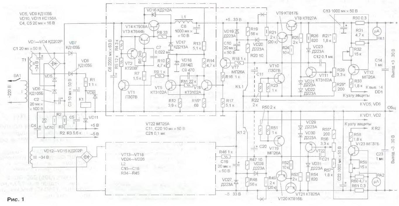
The circuit of the power source shown in Fig. 1. Dash-dotted line is highlighted the same nodes in both shoulders. Consider the operation of the device for example the source of positive voltage.
(click to enlarge)
The AC voltage of the secondary winding of the mains transformer T straightens diode bridge VD1-VD4 and filter capacitor Sat. Then the DC voltage is supplied to the switching transistor VT4 switching regulator and trigger Schmitt, collected on transistors VT5, VT6, the voltage of which stable parametric stabilizer R13VD18.
At the initial moment after turning on the power supply voltage sensor transistor VT7 is closed, the transistor VT5 Schmitt trigger open and the transistors VT1 and VT2 closed. The transistor VT3 is open, the current flowing through the emitter junction and resistors R6, R7. Consequently, the switching transistor VT4 is also open. Capacitor C8 begins to charge. The voltage across it increases as long until it becomes close to the set output. A further increase the voltage across capacitor C8 will lead to the opening of voltage sensor and VT7 triggering of the Schmitt trigger. As a result, the transistors VT1 and VT2 will open, and transistors VT3 and VT4 is closed.
Then the work included the inductor L1 To regenie inductance diode opens VD17, and the energy stored in the inductor is transferred to the load.
After depletion of the stored energy in the inductor diode VD17 is closed and the current in the load is supplied from the capacitor C8, the Voltage across it starts to decrease, and at some point will close the sensor voltage VT7. The Schmitt trigger will switch (transistor VT6 will be closed and the transistor VT5 is open), the transistors VT1 and VT2 is closed and the transistors VT3 and VT4 will open. The capacitor C8 will start again to charge.
Diode VD16 protects the switching transistor VT4 in emergency situations, for example, when failure of the diode VD17 or loss of capacity of the capacitor C6.
Compensation stabilizer transistors VT8, VT9, VT11 is assembled by simple the scheme and has no peculiar features.
For a smooth increase of the output voltage after switching on the power supply and prevent tripping when a significant capacitive load applied elements R19, VD20, C10. At the moment of switching the capacitor C10 is charged by two chains: through the resistor R19 and the resistor R21, the diode VD20. The voltage on the capacitor (and the base of transistor VT9) slowly over a period of about 0.5 s increases. Accordingly increases and the output voltage until the stabilizer is not enter steady state. Further, the diode VD20 closes and the capacitor C10 doseages through a resistor R19 to continue on the operation of the stabilizer is not affected.
Diode VD19 need for rapid discharge of the capacitor C10 after turning the unit off power and with decreasing output voltage. In this case, the voltage at the capacitor C8 decreases faster than C10 diode opens and VD19 the voltage on both capacitors is reduced at the same time.
In addition, to reduce the output voltage when the unit is turned off power applied to the relay K1. After turning on the unit in the network to relay K1 through the resistor R1 is energized from the rectifier diode VD7 VD8 Rectified the voltage is filtered by the capacitor C3 of small capacity. The relay is activated, it the contacts K1.1 open and do not affect the operation of the stabilizer.
When the unit is turned off the voltage on the capacitor C3 is disappearing faster than C6, therefore, the relay K1 is almost immediately releases its contacts K1.1 are closed and the capacitor C10 is quickly discharged through the resistor R20. At this point opens diode VD20 and the voltage at the base of the transistor VT9 is reduced almost to zero. The output voltage of the stabilizer is lost.
Chain R26VD23 serves for quick discharge of the capacitor C13 and capacitors in load when establishing a lower voltage. In this case, the voltage the collector of the transistor VT11 becomes smaller than the output voltage block, diode VD23 is opened and the capacitor C13 discharges through the circuit: resistor R26, diode VD23, plot the collector-emitter of the transistor VT11 and diodes VD21, VD22. In steady state circuit R26VD23 on unit operation is not affected.
The capacitor C12 prevents the excitation of the stabilizer. Capacitors C14 and C23 is connected directly to the output terminals of the power supply unit to reduce high-frequency fluctuations.
Chain R6C7 need to reduce the closing time of the transistors VT3, VT4. If the transistor VT3 is open, the resistor R6 is a voltage drop, plus applied to the base of the transistor. In the same polarity charging the capacitor C7. When the transistor VT2 is opened, through its section collector-emitter on bottom the scheme of the plates of the capacitor connected to the emitter of the transistor VT3. So by the way, to the emitter Board the transition of the transistor VT3 will be applied closing the tension that contributes to its forced closing, and hence the closing of the switching transistor VT4.
When triggered protection (overload or short circuit in the load), on base transistor VT10 through the divider R22R23 enters opening its voltage. In the result of the base of the transistor VT9 is connected to the common wire through plot the collector-emitter open transistor VT10. The voltage at the output of the block disappears.
Note the features of the construction sub-zero channel of the power supply. Pulse the stabilizer and the Schmitt trigger remains unchanged. Compensation stabilizer transistors of the other conductivity, and regulatory element VT21 in the circuit negative supply line. This simplified relationship compensatory stabilizer with node protection. Schmitt trigger (transistors VT17, VT18) is connected directly to the transistor VT20. Sensor function voltage transistor performs VT18 Schmitt trigger. So when you turn off the unit power output voltages disappeared simultaneously in both shoulders, used General relay K1 (contacts K1.2).
Node protection is fed from the bipolar voltage source. This allows a very just to control both shoulders PSU [3]. The negative voltage generates a multiplier diodes VD5, VD6 and the capacitors C1, C2 and at the level of -5 In stabilizes parametric stabilizer R2VD10.
Node circuit protection is shown in Fig. 2.
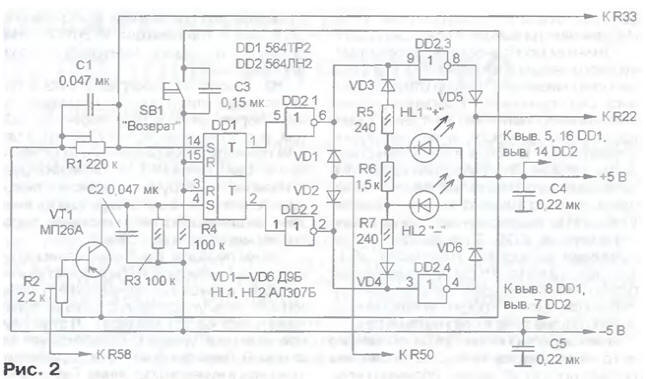
When the load current reaches the set value, the voltage drop across the resistor R30 (see Fig. 1) will be sufficient for opening the transistor VT12. The input S (pin 14) of the trigger DD1 goes to a high level, and it will switch to one state. The output inverter DD2.1 appears a low level through the diode VD1 and resistor R50 affects the transistor VT19 (see Fig. 1) that will lead to the opening the last and closing composite transistor VT20VT21. The output voltage sub-zero source will be lost.
The output of inverter DD2.3 will be a single signal, acting through diode VD5 and a resistor R22 (see Fig. 1) on the transistor VT10, which generally leads to closing and positive shoulder. Led HL1 "+" indicates the presence of overload it in plus the shoulder of the power supply. Similarly, the protection node works and in case of overload negative source.
Thus, wherever any overload, off both shoulders stabilizers, and this condition will persist indefinitely until button is pressed SB1 "Return". In this case, a high level affects the inputs R (findings 3 and 15) and switch the triggers in the zero state. The efficiency of the stabilizers will be restored. The capacitor C3, shunt contacts button SB1 to set the triggers to the zero state at the time switching the unit to the network. Resistors R1, R2 are used to set the level sensitivity of the protection. Capacitors C1, C2, shunt inputs S triggers, prevent false triggering node protection from surges induced in the connecting conductors. Diodes VD1-VD6 need for decoupling output circuits.
Mains transformer in the power supply you can use either providing the necessary power. In the author's version used the finished transformer TC-180-2. The primary winding is left unchanged. It contains 680 turns the PEV-1 0,69 All secondary windings are removed, and in their place new wound winding II and III, containing 105 turns of PEV-1 to 1.25. Transformer can be made independently on the basis of the magnetic PL h.
Inductors L1 and L2 are wound on armored cores B-30 ferrite MNM. Coils contain 18 turns harness composed of nine wires sew-2 to 0.4. The gap between the halves of the magneto rovada to 0.2 ..0.5 mm.
Diodes CDR (VD1-VD4, VD12 - VD15), placed on a small heatsink, you can substitute other, suitable for direct current no less than 3 A necessary and reverse voltage. Instead of diodes KD105B (VD5-VD9) and DA (VD19-VD23, VD27-VD31) it is permissible to use any of the series KD, KD. Diodes DB (VD1-VD6, Fig. 2) any of the interchangeable series KD521, KD522.
Relay K1 - RASA performance RS4 590 202 on the operating voltage of 12 V. Better to pick up relays at higher voltage, for example, RESA performance RS4.590.207 voltage of 27 V. In this case, you should use a current limiting resistor R1 least resistance and power.
Transistors CTB (VT3, VT15) interchangeable on CTA, CTU, at least on CTV, CTG or CTV, CTG. In place of transistors VT1, VT10, VT13 it is permissible to use any silicon with allowable voltage the collector-emitter of at least 60 V. Instead of transistors MPA (VT7, VT12, VT19, VT22 and VT1, Fig. 2) you can apply any of the series E, MP; instead CTA (VT5, VT6, VT11, VT17, VT18) - KTV-CTE, CTB. Transistor CTA (VT8) replace any of this or from CT and CTA, CTG, transistor CTA (VT21) - any of this or from CT and Instead CTG transistors CTA (VT4, VT16) it is better to apply with greater peak CTA the collector current.
Transistor MPB (VT23) should be selected according to the maximum voltage collector-emitter because it is on the border of the valid values.
Transistors VT4, VT8, VT16, VT21 and diodes VD17, mounted on a small VD25 heat sinks dimensions respectively 50x50x5 and 40x30x3 mm.
Chip series 564 interchangeable corresponding series C.
Oxide capacitors C6 and C15 composed of two K50-24 and two 1000 UF K52-1B 100 µf, all voltage 63 connected in parallel. Capacitors C1, C2, C10, C11, C19, C20 - C50-6, C3, C4, C5, C13, C22 - C50-16, C12, C14, C21, C23 - K73-17.
Microammeter RA1, RA - M to 100 µa. All parts of the device in advance check it out. In the original power source is assembled on multiple boards mounted Assembly.
When establishing the unit it is best to use an oscilloscope. It is connected to the emitter of the transistor VT4. The engine resistor R28 to establish a middle position, and the resistor R22 is temporarily fed. Include the power supply to the network. On the emitter of the transistor VT4 should appear rectangular pulses. If the voltage is missing, first and foremost, you should make sure that the relay K1 worked. Otherwise, the selection of the resistor R1 are making to relay worked at minimum line voltage (190). After this measure voltage collector-emitter transistor VT8. It should be in the range of 1.5 to 2… In and stored by a change of the output voltage.
Switching switching regulator occurs when the voltage the collector-base of transistor VT9 is approximately equal to 0.9 V. If it is necessary increase in the emitter circuit of the transistor VT7 should include one or more diodes in the forward direction. The switching frequency to a small extent dependent on the resistors R17 (with its decreasing frequency decreases) and R15 (with it increases the frequency decreases).
Resistors R27 and R29 are selected minimum and maximum values of the output voltage (3 and 30).
Now to the output of the stabilizer connects the load (or its equivalent) resistance of about 3 Ohms power not less than 27 watts, pre-installing the output voltage is approximately 5 V. Gradually increasing the output voltage, ensure that the load current does not exceed 3 A. in addition, it is necessary to control the shape of the pulses. If the duration of the pauses between the pulses will be less than 1/5 period, any failure of hesitation. In this case, it is necessary to increase the inductance of the inductor by applying a magnetic core is a large or increasing the number of turns.
Then calibrate the ammeter, which measures the load current. To measure the voltage at the output of the power supply unit can include microammeter with incremental the resistor has a resistance of about 300 ohms.
Next, solder a resistor R22. The engine of the resistor R32 is installed in the upper ( scheme) position, and the resistor R28 - minimum voltage. To the exit the stabilizer is connected by a resistor 40 Ohms. Include the power supply in network and increasing the output voltage, set the load current of 250 mA. Then resistor R1 (see Fig. 2) ensure the protection tripped and joined led HL1. For the source of negative voltage minimum current protection operation set by resistor R2.
After that, the engine of the resistor R32 is moved to the lower (on) position. The load resistance is reduced and establish a current of 3 A. Moving the engine resistor R32 up (the scheme), notice the time of fault. Now you should measure the resistance out part of the resistor R32, put the resistor is close to the nominal value and to calibrate its current tripping.
Similarly, adjust the shoulder sub-zero voltage.
In conclusion, measured by the oscilloscope voltage ripple at maximum current load. If the ripple exceeds 30 mV, install additional the capacitors C11 and C20 (Fig. 1 shows dashed lines). Can to be that by quickly turning the engine resistor R28 (R56) output the voltage still varies, although the engine is stationary In this case, the upper the output resistor R21 need to unsolder and connect with the collector of transistor VT4 (shown by a dotted line). Lower terminal of resistor R49 should also unsolder and connected to the junction point of elements R2, C2, VD6 (see Fig. 1). Resistance resistors R21 and R49 should be increased to 20 ohms.
The efficiency of compensatory stabilizer can be increased if VT8 and VT21 to use transistors with a lower saturation voltage collector-emitter, taking into account the recommendations [4].
Instead MPB (VT23) it is better to use a germanium transistor with a large allowable voltage collector-emitter, for example, GTV, GTG.
Literature
Author: Balashov, Shadrinsk, Kurgan region.