


")

In the practice of Amateur radio from time to time it becomes necessary to stabilized DC voltage exceeding traditional 5…15 V, used to power the equipment on the chip. In such cases, will help the described device.
Technical characteristics of the source
- The intervals of the output voltage, ......5…55, 50…100
- Maximum output current, mA......200
- The restriction level output current, mA......250
- Output voltage ripple, mV, not more......10
- The instability of the output voltage when the supply voltage within 190…240 V and output current 0…200 mA, %, not more......0,1
High stability is ensured by the application as a source of model the voltage amplifier and the error signal of the chip CREA[1].
The circuit of the power source shown in Fig. 1. The rectifier is assembled to the circuit of the voltage doubler diodes VD1 and VD2, which is to reduce switching noise is shunted by the capacitors C1 and C2. To reduce the power dissipated in the transistors of the stabilizer, when working in the interval 5…55 To cut off a portion of the secondary winding of the transformer T1, the switch SA2.
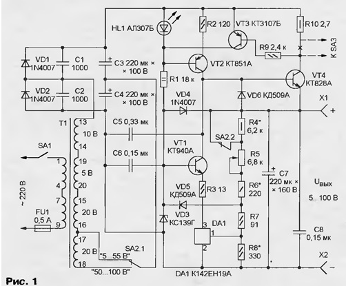
The VT2 transistor serves as a current generator. The voltage at its base is stable led HL1, the value of the collector current (8…9 mA) is set by a resistor R2. Through the divider of the resistors R4-R8 part of the output voltage of the stabilizer is supplied to the control input of the circuit DA1. If the voltage here is less than 2.5 V, the anode the current IC and the collector current of transistor VT1 not exceed 0,4 mA. Thanks this transistor connected in the common-base circuit, the voltage at the anode circuits DA1 does not exceed 3.3 V, and it dissipated power does not exceed valid value.
In this mode almost all the collector current of the transistor VT2 comes in base transistor VT4, opening the latter. The output voltage of the stabilizer and the control input circuits DA1 growing. When the latter reaches 2.5 V, the anode current DA1, and the collector current of the transistor VT1 will increase dramatically, the base current transistor VT4 will decrease and the output voltage of the source will be stable at a level determined by the ratio of the resistances of resistors R4-R8. Smoothly regulate the output voltage of the variable resistor R5, the interval adjust select switch SA2.
The normally closed transistor VT3. But with the increase of the load current and collector current of the transistor VT4 to about 250 mA voltage drop across the resistor R10 reaches the value at which the transistor VT3 open, led sunterra HL1. This leads to a decrease of the collector currents of transistors VT2 and VT4. In the result of the output current of the regulator is limited to the above value. About the operation of the current limiter can be judged by the decrease in brightness the illumination of the led.
When the result of the action of the limiter output voltage stabilizer will drop to about 2.7 volts, the current through the circuit HL1R1 current going to the load through opened the diode VD4, some increasing the total of the flowing current. If diode VD4 was not, as a result of changing the polarity of the applied voltage open-collector junction of transistor VT1 and the current through R1, directed to the base of transistor VT4. As a result of the amplification transistor VT4 the increment of the load current would be much higher.
It is possible to fully remove the effect of increasing the current through the diode, included in the open circuit connecting the collector of transistor VT1 base transistor VT4 and the collector of the transistor VT2. But in this case, the transistors VT1 and VT2 cannot be installed on a common heat sink without the insulating strips.
It should describe the purpose diodes VD5 and VD6. Assume that the switch SA2 is in the "50…100", and the output is minimum voltage (engine, variable resistor R5 in upper circuit position). After the transfer switch SA2 in position 5…55 V" voltage 50 V to which capacitor C7 is charged, is applied to the resistors R6-R9, with more than half (about 30 In) - to the control input of the circuit DA1. Last down will not work, but the internal circuitry of the chip is the voltage get on the anode and the emitter of the transistor VT1, closing the latter. In the collector current of the transistor VT2 will flow to the base of transistor VT4 and the output of the stabilizer appears to the maximum possible voltage. To unfortunately, this state is stable and self-stabilizer exit you can't.
Diode VD5 is used to avoid such critical situation. Opening, he limits the voltage on the input circuit DA1 is a valid value. Correct the choice of the voltage stabilizing Zener diode VD3 and the resistors R7 and R8 guarantees that in normal mode, diode VD5 remains closed and does not affect the operation of the stabilizer.
The sudden change of position control in the direction of decreasing the output voltage is possible that due to the slow discharge of capacitor C7 the voltage at the emitter of the transistor VT4 "lags" the voltage at its basis. There is a danger of breakdown of the emitter-tion of the transition voltage of the transistor, attached in the opposite direction. Diode VD6 prevents this reversible, but unwanted breakdown. Capacitor C7 is discharged through the circuit VD6, VT1, R3, DA1. Due to the resistor R3, the discharge current does not exceed 100 mA.
In the power supply applied unified transformer TP-127/220-50 [2] overall power output of 60 watts. Such transformers have less power too large for the proposed device active impedance the windings. To reduce some of the stress on the secondary windings transformer the conclusions of its primary windings connected in a non-standard way. When independent manufacture of the transformer should focus on these in Fig. 1-circuit voltage of the secondary winding. Section winding wires must be large enough resistance windings were about the same as the specified transformer: 1-9 - 56 Ohm, 13-16 -2,3 Ohm, 17-18 -1,3 Ohms.
All fixed resistors in the device - S2-23 or MLT appropriate power, R5 - PPV-40. Capacitors C1 and C2 are ceramic, for a voltage not less than 160, for example, km-5 group TKE no worse M1500. C3, C4, C7 - import analogues C50-35, C6 - km-5 km or-6, C5 and C8 - K73-17 for a voltage of 250 V. the Diodes 1N4007 have home analog KD243ZH, you can use any diodes for voltage not less than 200 V and 300 mA. Instead KDE you can install any diodes with permissible pulse current of 300 mA.
The transmission of the current h21e all power transistors must be at least 30 with this parameter of the transistor VT4 should be checked when the collector current 200 mA. Replacing the transistors VT1, VT2 and VT4 must be selected with utmost voltage collector-emitter of not less than 160 and the allowable current collector is not less than 100 mA (VT1 and VT2) and 1 A (VT4). The transistor VT3 - any silicon low-structure p-n-p. Led HL1 - any visible radiation. To to maintain a constant collector current of the transistor VT2 when installing LEDs HL1 green or yellow, you may slightly increase the value resistor R2. Chip CREA you can replace imported analogue of the TL431.
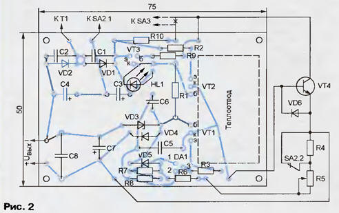
The main part of the details of the power source is placed on the PCB size 50x75 mm of fiberglass with a thickness of 1.5 mm (Fig. 2, a side view of the printed conductors). It is also a common finned heat sink transistors VT1 and VT2 sizes 20x24x38 mm Transistor VT4 is mounted on a separate ribbed heat sink dimensions 36x100x140 mm Diode VD6 soldered directly to the findings of this transistor.
Connect the assembled device to the network the first time, preferably through laboratory adjustable autotransformer, the output of which is pre - there will be a zero voltage. The slider of the variable resistor R5 should to be in the position of minimum resistance, the switch SA2 - in position "5…55". To the output of the source, connect a voltmeter and make sure that as rotation of the handle of the autotransformer in the direction of increasing voltage the voltmeter grow, but, reaching approximately 5 To remain at this level. If so, you can bring the input voltage to a nominal 220 V and check the voltage on some elements of the device. The cathode of the Zener diode VD3 it should be close to the voltage stabilization (3.9 In), on top the scheme output resistor R7 is approximately 3.3 V. the voltage Drop across the resistor R2 should be about 1.1 V, if it is greater, should be increased the value of the specified resistor so that the current through it, the current was in 8…9 mA.
Resistors R4, R6, R8 are selected in the following order. When the switch SA2, at 5…55 V", set with AC resistor R5 maximum output voltage source. Choose the resistor R8 so it was a little more 55 V. Translate the slider to the resistor R5 in the other extreme position, and, picking up resistor R6, achieve output voltage slightly less than 5 V. Then translate the switch SA2 in position "50… 100 In" and choose the resistor R4, achieving the specified limits of adjustment output voltage of the resistor R5.
Be sure to check the operation of the power source with the maximum load. If at any range with a maximum output voltage of the increase the load current leads to a decrease of this voltage, in case of insufficient the voltage corresponding to the secondary winding or too large the resistance of the windings.
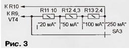
Milliammeter to control the output current can be enabled to break the wire, coming from the emitter of the transistor VT4 to other circuit elements (except diode VD6). Since using the device in this case, in addition to the load current will flow and the current divider R4-R8, the meter should be set to zero adjusting screw when operating without load source. The device can be supplemented by the switch-level output current limit (Fig. 3). The resistance introduced part of the chain of resistors R10-R13 must be so that, when the current limit on it fell a voltage of about 0.6 V.
A voltage regulator as shown in the diagram is easy to calculate for any the adjustable range of output voltage with an upper limit of 50…500 V. Transistors (except VT3) should be selected from approximately-fold margin voltage relative to the maximum output. The current generator transistor VT1 should produce a current of about 1.2 times greater than the maximum output current stabilizer, divided by the coefficient h21e transistor VT4. When the calculated the output current is more than 1 And as VT4 required a composite transistor. Currents through the resistor divider R1 and R4-R8 can be selected in the range of 4…10 mA. If stabilizer design for fixed or adjustable within a narrow range of the output voltage, the diode VD4 and VD6 can not install.
Literature
Author: S. Biryukov, Moscow