


")

The power supply is designed to power portable TV and radio. Its nominal output power - 20 W, and the efficiency at rated output - at least 85%. Working frequency conversion - 68 kHz.
Unit features optimized for load lying in the range 0,5…1 of nominal power. He is stable when changing the mains voltage in the range of from 170 to 240 V, can withstand short-circuit (fault current measured by avometra V7-35, equal to 6 (A).
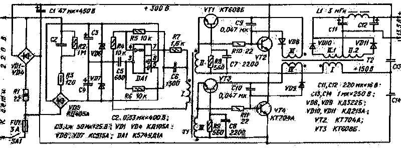
Schematic diagram of the unit shown in Fig. 1. The master oscillator inverter is assembled by operational amplifier DA1 covered by the chain of positive operating system. Load the OS serves as the primary winding of pulse transformer T1. The differentiating circuit R7C6 creates uprated front switching transistors VT2 and VT4.
The node that provides the acceleration of the process of resorption of minority charge carriers in these transistors, consists of elements VT1, VT3, VD8, VD9, R8. R9, C7-C10 and additional windings III, IV transformer T2. Consider the work site on the example of the upper circuit on the shoulder of the half-bridge inverter.
Let the transistor VT2 is open and saturated. In this case, the transistor VT1 is closed to him and the applied voltage is about 6 In from the winding III of the transformer T2. Capacitor C9 is charged.
At the end of halftime changes abruptly switching the polarity of the voltage at the output of the master oscillator and, therefore, on all windings of the transformer T1; LI¦ - the voltage on the primary winding of the transformer T1. Transistor VT1 open, and thanks to the differentiating circuit R8C7 this process occurs rapidly.
Under the influence of the total voltage winding III of transformer T2 and II of the transformer T1 starts the rapid resorption of minority charge carriers from the base of transistor VT2 circuit: winding III of transformer T2, the collector junction of transistor VT1, winding II of the transformer T1, the emitter junction of transistor VT2, diode VD8. After a time, tpac, there is a sharp decrease of the collector current of the transistor VT2. In this case, the transistor VT4 is in the process of opening.
The voltage on the windings of transformer T2 reverses its polarity. The charge accumulated by capacitor C9, supports closing the base current of transistor VT3 before it is completely closed. From this point, the reverse voltage on the emitter transition VT2 is reduced to a value not exceeding 1 In that a positive impact on the reliability of the inverter.
As a switch, except indicated in the diagram, you can use transistors CTB, CTV, as well as any of the series CT; other suitable high voltage low and medium frequency transistors. It is desirable to install the heatsink with the effective scattering area of about 50 cm2. Transistors VT1, VT3 - any silicon with maximum permissible pulse current collector is not less than 500 mA and a cutoff frequency of at least 100 MHz.
Oxide capacitors C1, NW, C4 - C50-12. C50-27; C11, C12-C50-29, K53-25, K53-28; other - any ceramic, glass or glass-ceramic. The capacitor C5 must be group TKE rltb, MZZ or M47. The resistor R1 is C5-16, the rest of the IFL.
The transformer T1 is wound on an annular magnetic core size CHH,5 ferrite 2000NM. Winding I made wire sew-2 contains 0.1 and 52 of the coil, the winding II and III - 8 turns of the same wire. Transformer T2 is also wound on the annular magnetic core size CHH ferrite 2000NM 1-A. Winding I contains 120 turns of wire sew-2 0,25, winding II - 2x12 turns of wire sew-2 0,8, winding III and IV - 5 turns of wire sew-2 0,25. The inductor L1 is made on an armored magnetic Sh5h5 ferrite 700NM. The coil has 50 turns of wire sew-2 to 0.8. Between the halves of the magnetic core of the inductor is necessary to enclose the strip of thick paper with a thickness of 0.3 mm.
An overall power transformer T2 on the conversion frequency of 68 kHz is 42 watts, allowing you to increase the power output of the power source to the specified value. To do this, its winding I, III, and IV must be wound wire sew-2 0,41, winding II, and the winding of the inductor L1 - wire sew-2 1. In addition, it is necessary to increase the area of heat sinks transistors VT2, VT4 roughly in half, to convert the capacitance of the capacitors C1,C11,C12 and the inductance of the inductor L1 in accordance with the recommendations outlined in [3]; the resistance of the resistor R7 should be reduced to 680 Ohms, R1 - to 10 Ohms.
There may be a need to "umamani" of the operational amplifier DA1 additional transistor stage current amplification, as well as to increase the capacitance of the capacitors C2, Sat.
Assembled construction must be placed in a shielding box. Author's design for the unit has dimensions of HH mm, which corresponds to a power density of about 105 W/m3. With error-free installation and operational details of the source does not require establishing and begins to work immediately.
Literature
1. Biryukov C. the power supply for Radio-86RK. Radio, 1990, vol. 7, pp. 58-61.
2. Tsvetayev C. power supply. Radio, 1990. No. of 9.0.59-62.
3. Eranosian S. A. power supplies with high-frequency transducers. - Moscow: Energoatomizdat, 1991.
Author: V. dorozynski, Gelendzhik; Publication: N. Bolshakov, rf.atnn.ru