


")

The device stabilizes the voltage of load limits and consumed current, passing in the constant current mode. Pulse mode operation provides high efficiency at all operating conditions. The device is not afraid continuous output circuits. It can serve as a source of current for electrolysis, electroplating processes and others that require a stable or limited current. The device can be used for charging almost all types. In Amateur literature published many descriptions of laboratory power supplies. The proposed source has a broad functionality, simplicity, high efficiency. In Fig. 1 shows a functional diagram.
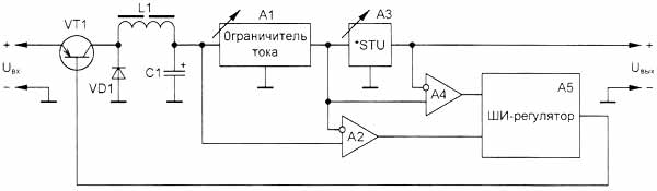
Fig. 1
The unit step-down voltage regulator with PWM control on the switching transistor VT1. After the cumulative elements of the inductor L1 and capacitor C1 are connected in series adjustable linear current limiter A1 and the voltage regulator A3. Diode VD1 provides a flow of current of the inductor L1 to the capacitor C1 and the load when closed switching transistor VT1. The load current is limited from above by a node A1 from 10 mA to 5 A. a voltage Regulator A3 allows you to adjust the output voltage from 0 to 30 V. the Differential amplifiers A2 and A4 with a gain of about 5 monitor the voltage drop across the blocks A1 and A3. When at least one of them is too high, the switching transistor VT1 is closed by a signal pulse-width controller A5. This is achieved by high efficiency and stabilization of not only the output voltage and current. Small power dissipation in the regulatory elements increases the reliability of the device allows to reduce its weight and size by reducing the size of heat sinks compared with linear regulation. In Fig. 2 shows a schematic diagram of the device.
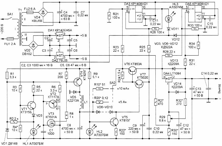
Fig. 2
Components VT4, VD5, L1, C8 correspond to VT1, VD1, L1, C1 in Fig. 1. The elements VT1-VT3, C1, VD3, HL1, R3-R8 assembled a pulse-width controller A5. The current limiter A1 compiled by the regulator circuit current at the transistor VT6 and VT7, diode VD6-VD10 and resistors R10-R20, one of which connects the switch SA2. Adjustable voltage regulator A3 assembled on a chip DA4. Differential amplifier A2 (see Fig. 1) high voltage Oh CRUD (DA3) with resistors R21, R23, R25, R26. A similar differential amplifier A4 - DA5, R28, R31.R33, R34.
Reduced to 30 In the transformer T1 network voltage winding II diode bridge rectifies the VD4 and smoothing capacitor C4. This voltage (about 40 In) - input for switching regulator. The resistor R1 and the Zener diode VD1 form a parametric voltage regulator power master oscillator, which is made on the unijunction transistor VT2. The transistor VT3 - current amplifier master oscillator. The selection transistor CTG as switching (VT4) due to its high reliability and wide availability. The generation frequency of 40 kHz is selected in accordance with the frequency properties of the transistor CTG. The resistor R2 and the led HL1 assembled parametric voltage regulator In about 2 for fixing the voltage level at the emitter of the regulating transistor VT1. Diode VD3 prevents the flow of reverse voltage at the emitter junction of this transistor. Opening, the switching transistor VT4 connects the inductor L1 to the output of the rectifier diode bridge VD4. Flowing through the inductor L1 current charging the storage capacitor C8. Changing the voltage on the base of the transistor VT1, you can adjust the width of pulses opens the transistor VT4, and the voltage on the storage capacitor C8. The current limiter A1 is made discrete.
Avoiding the use of chip LT1084 due to its high enough maximum input voltage (37 In). Furthermore, the use of discrete element increases efficiency. The voltage drop across dakotadome resistor integral stabilizer equal to 1.25 V, at a current of 5 A at this resistor dissipates power of 6.25 watts. The applied current limiter the voltage drop across dakotadome resistor UR equal to the difference between the voltage drop across the diode chain VD6-VD10 and voltage base-emitter composite transistor VT6VT7. In this case UR is approximately equal to 0.6 V. the Power dissipated in the resistor R20 (at the limit 5 (A), approximately equal to 3 watts. Resistance dakotadome resistor R is calculated by the formula R=UR/I, where I is the desired current limit.
In the instance of the author implemented 11 limits the current-limiting: 10, 50, 100, 250, 500, 750 mA; 1, 2, 3, 4, 5 A. They correspond to the resistors R10-R20. Since the voltage across capacitor C8 varies, the current through stabistor composed of diode VD6-VD10, determines the stabilizer transistor VT5 and led HL2. Resistor R22 in the emitter circuit of the transistor VT5 set the current through the circuit VD6-VD10 within 10…12 mA. Adjustable voltage regulator A3 is made on the chip DA4. Diodes VD13, VD14 enhance its reliability. Through these diodes when you unplug the PSU from the mains discharged the capacitors C12 and C13, eliminating the excitation of the stabilizer.
To obtain zero output voltage in the circuit of the control electrode through a divider R27R30 voltage of negative polarity regulator from DA2. Rectifier diode bridge and VD2 integral stabilizers DA1, DA2 also nourishes digital voltmeter on the chip CREW collected according to the standard scheme. The output signals of operational amplifiers DA3 DA5 and through the diodes VD11 VD12 and come to a common load resistor divider R3R4. Led HL3 displayed on the front panel and indicates the transition of the power supply unit in the restriction mode constant current. The increase in the voltage drop across the current limiter or voltage regulator causes an increase in voltage across the resistor R4. When it exceeds a threshold value (about 3 In), opens the transistor VT1, shortening the pulse generator transistor VT2.
Design and details
The PSU is mounted in body size 90x170x270 mm Transistor VT4 and diode VD5 installed without insulating strips on one heat sink area of 200 cm2. On the heat sink area of 400 cm2 mounted transistor VT6 (through the insulating spacer and stabilizer DA4. To improve thermal stability of the diode VD6-VD10 advisable to install the heat sink as close as possible to the transistor VT6. The device is assembled on a universal breadboard, PCB has not been developed. The transformer T1 is made from the mains transformer tube TV.
The magnetic core is disassembled, remove the coil. Coiled filament winding (they are located in the upper layer and a wound wire of the greatest diameter), counting the turns. Multiplying this number of turns 5, we get the number of turns of the winding II. Then fully wound on both the anode winding coils on a single spool. Then, for each coil is wound in bulk half the number of turns of the winding II in the two wires of the anode winding. Wire diameter 0.8 mm anode winding corresponds to the cross section of 0.5 mm2. Winding two wires gives an equivalent cross-section of 1 mm2, which allows to obtain a load current of 5 A.
Multiplying the number of turns of the filament winding 3, we get the number of turns of the winding III. This winding is also in the two wires can be wound on one of the two coils. In connection with small consumption of current from winding III asymmetry of the magnetic field of the transformer is obtained is irrelevant. After Assembly of the magnetic circuit Polubotko III are connected in-series with regard to phasing, the beginning of one Polubotko III is connected to the other end, forming a branch of the middle. The inductor L1 is wound on the yoke B ferrite NM in bulk in the two wires of the anode winding to fill the frame. To create a non-magnetic gap between the nested cups textolite washer with a thickness of 1 mm. After tightening the bolt MB ready choke impregnated with BF-2. Drying and curing of the adhesive was carried out in an oven at a temperature of 100 °C.
At independent manufacture of the throttle at the other magnetic circuit, it should be borne in mind that the current through the inductor has a triangular shape. Average current consumption 5 A corresponds to the amplitude of 10 a, While the current of the magnetic circuit should not enter saturation. The LT1084 regulator (DA4) can be replaced by domestic analogue CREA. Variable resistor R29 to make them more durable wire used PPB. Considering that a switch SA2 significant current flows, to improve the stability and durability of applied ceramic disk switch PN, the contacts are connected in parallel. Svetodiodnom (HL3) can be replaced by foreign L-543SRC-E.
Establishing
The selection of resistor R30 establish a zero output voltage at the output of the power supply at the bottom on the diagram the position of the slider of the variable resistor R29, and the selection of the resistor R32 - voltage 30 V At upper circuit on the position of the slider R29. Connect a voltmeter to the terminals 2 and 3 of the stabilizer DA4 and selection of resistor R4 set the voltage to 1.5 V. At the time of establishing perhaps the use of trimming resistors. But their use for continual use is not recommended due to the instability of the resistance of the movable contact system. Then connected to the output terminals of the load through the ammeter.
Changing the resistor R29 output voltage, built-in ammeter and voltmeter to monitor the output parameters. At low-limits due to the presence of currents control stabilizer DA4 will require adjustment of the resistors R10-R12 compared with the calculated value. The led on HL3 need to check the current limit and stability on all ranges. The proposed laboratory power supply is very comfortable to work with, including the charging of batteries from 7D-0.1 to starter car. Built-in digital voltmeter set the final charging voltage, the switch SA2 select the required charging current and connect the battery (the battery). Charging is stable current, when the preset battery voltage, charging is terminated. For three years of operation of the proposed device failures in his work was not.
Author: K. frost, Nadym, Yamal-Nenets Autonomous. County; Publication: www.cxem.net