


")

Low frequency power sources in power transformers, because of its large size and mass, and also low efficiency everywhere are forced out of impulse. The development of powerful high-frequency transistors and pulse transformers on ferrite the cores allows you to transfer energy to the load at frequencies commensurate with length of radio waves, and to bring the weight and dimensions of such sources to minimum quantities.
The proposed source is designed to supply a powerful apparatus and charging car batteries. Source built on the basis of a single Converter, comprising a master oscillator at unijunction transistor and the blocking oscillator powerful bipolar transistor.
The principle of operation of the source based on 3 times the conversion voltage.
AC mains voltage is rectified (converted to DC high voltage) and serves to key the transmitter. High-frequency key the transformer converts the DC voltage in low-voltage pulse. The latter is rectified and is supplied to the load.
In flyback converters (inverters) in the period of the closed state a transistor switch is the accumulation of energy in the transformer, and its transfer in the load occurs when the open key. In such a unipolar inverters the magnetization of the transformer leads to residual magnetization of the ferrite core, and to reduce the required non-magnetic gap in the magnetic circuit.
The energy stored in the transformer during the time of the switching pulse, not always manages to dissipate during the pause, which can lead to saturation the transformer and the core loss of magnetic properties. To eliminate this effect the primary circuit the transformer is shunted by high-speed diode with a resistive load.
The source circuit shown in Fig.1.
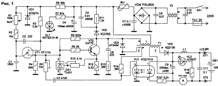
Switching noise in switching power supplies arise from switching the operation mode of powerful regulatory elements. To protect network and the Converter from surges installed a surge protector for winding the inductor T2 with capacitors C7, C8, C10 to suppress nesimmetrichnykh interference.
Limitation charger current of the filter capacitor C4 is performed on the PTC Rt1, the resistance of which decreases with increasing temperature. Impulse noise Converter, occur when switching switching transistor VT2 and transformer T1, parallel circuits are eliminated VD2-C5-R11 and C6-R13, interference in the load circuit are suppressed by the inductor L1. The duration pauses between the pulses of the output current in this case is slightly increased, but not impairs the conversion.
The pulse shaper of the inverter is made on unijunction transistor VT1. The voltage VT1 stabilized diode VD1. Charger the voltage on the capacitor C1 periodically opens VT1 and creates the resistor R4 sequence pulses with a frequency determined by the values of R1, R2 and C1. The capacitor C2 accelerates the transition process of switching transistor VT1.
When power is DC (rectified by a diode bridge VD4) the filter capacitor C4 through the winding 1 of the transformer T1 is supplied to the collector transistor VT2, which aggregates the blocking oscillator. The flow of collector current through the winding 1 T1 is accompanied by the accumulation of energy in the magnetic field of the core. Pulse the voltage from the resistor R4 opens the transistor VT2 on few microseconds, the collector current in VT2 this time increases to 3…4 A. After the end of the positive pulse current the collector terminates.
The cessation of current causes the appearance in the coils of the transformer EMF, which creates in the winding 3 impulse voltage. Diode VD5 with capacitor C9 rectify and filter the voltage through the inductor L1 is supplied to the load.
Impulse voltage with winding 2 T1 through resistors R5, R9, R14 is supplied to the base of transistor VT2, and the scheme goes into self-oscillation mode. Capacitor C3 maintains stability the operation of the blocking oscillator.
Stabilization of the output stress is the optocoupler VU1, providing galvanic isolation of high-voltage and output-low voltage circuits. The increase of the load voltage, for example, by to increase resistance, turn on the led of the optocoupler VU1, photodiode which opens and bypasses the signal from the coil 2 T2. Pulse voltage at the basis of VT2 is reduced, accordingly, decreases the time of the open state. The duration positive pulses in the winding 3 T1 also decreases, which causes a decrease in output voltage and charging current of the battery GB1). When the reduction of the load voltage, the above process is reversed.
In case of over current of the transistor VT2 is increasing pulse voltage the resistor R12 in the chain of its emitter. Then open parallel a voltage regulator DA1 and bypasses the base voltage VT2. Thereby also decreases the duration of the open state (up to a breakdown of self-oscillations). The current cut-off transistor VT2 is adjusted resistor R10.After eliminate the overload start occurs in the blocking oscillator from pulse shaper on VT1.
The choice of a high-frequency transformer depends on the load power. Power the transformer depends on the frequency of the oscillator and ferrite materials. When the increased frequency of 10 times the output of the transformer is increased by a factor of 4 times. Due to the complexity of the independent production of pulse transformer in the device used a transformer from a legacy monitor. Suitable transformers and from the TV. For reference, here is sample data of the transformer T1. Core - BM with a gap in the Central the stud. Winding 1 contains 56 turns of wire sew-2 0.51 mm, winding round 2-4 0.18 mm, winding 3 -14 turns bundle of 3 wires 0,31 mm.
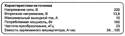
The device is assembled on the PCB size mm 115x65 (Fig.2).
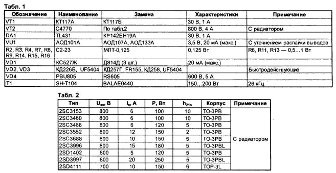
The jumpers are located from the electronic components. Radiator key transistor VT2 is used on the processor of the computer. For better cooling, you can apply the fan from computer power supply by connecting it to a source output through a resistor resistance 33…56 Ohms. The types of elements contained in table.1, it is possible replacing the transistors of the Converter - in table.2.
Commissioning collected schemes begin with a thorough inspection of the Board. In the gap network the wires include a light bulb 220 In any capacity, instead of the load - automotive light bulb (12 V, 20 candles). For defective parts and errors in the installation of network the light bright light, and the car does not burn. If the scheme is defective, network led is not lit or lit a faint glow, and automobile and bright. The brightness of the lamps in the load (output voltage) can be adjusted resistor R1. The threshold of protection from overcurrent set the resistor R10, the voltage (at maximum load) adjustable resistor R5. The Selection R15 (if necessary) adjusted current of the led of the optocoupler in VU1 5…6 mA.
In the presence of the oscilloscope is convenient to first check the operation of the generator at transistor VT1, filing for the inverter power supply voltage 30…50 V from a laboratory source. The frequency the generator can be adjusted by resistor R1 or the capacitor C1.
With a weak inverse connection (high resistance R5) or an incorrect connection of the winding 2 T1 blocking oscillator to VT2 may disconnect from overload and short-term re not start.
Authors: V. Konovalov, A. Vanteev Creative laboratory Automation and telemechanics", Irkutsk