


")

In Amateur radio magazines of circuit switching power supplies a power greater than 500 W is uncommon. And therefore was developed pulsed stable power source with the following parameters:
The power delivered in the load 1 kW The output voltage ±50 V Maximum current in the load 10 And The output voltage at maximum current (not less than) +48 V The current response protection about 14 And Frequency conversion 50 kHzSchematic diagram of the pulsed power supply (UPS) is shown in Fig. 1.
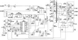
Fig. 1 (click to enlarge)
The basis of the scheme is put the chip DAI TL494CN family of controllers with pulse-width modulation. This chip used in computers and UPS has been very successful. Consider her work in the Converter circuit in more detail. TL494CN includes an error amplifier, built-in adjustable oscillator, a comparator adjust the "dead" time, trigger control, a precision reference voltage source (ION) and 5 IN the control circuit output stage. The error amplifier generates common-mode voltage in the range of 0.3…2 V. the Comparator to adjust the "dead" time has a DC offset, which limits the minimum duration of the dead time the value of the order of 5% of the duration of the output pulse. Independent output shapers transistors provide operation of the output stage in the common-emitter circuit. The current of the output transistors of the chip - up to 200 mA. TL494CN operable at a voltage of 7 to 40 V. In Fig. 2 shows a circuit of the chip and the structural layout of its internal circuits.
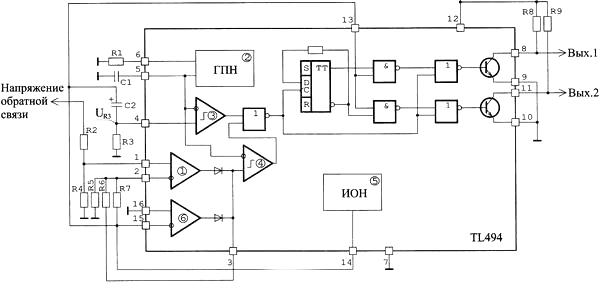
Fig. 2
When power is triggered sawtooth generator 2 and the reference voltage source 5. The sawtooth voltage from the output of the generator 2 (Fig. 3,a) is fed to the inverting inputs of the Comparators 3 and 4. To the non-inverting input of the comparator 4 receives voltage from the error amplifier 1. Since the output voltage of the power supply at this point are not yet available, the feedback signal from the divider R2R4 to the non-inverting input of the error amplifier is equal to zero. To the inverting input of this amplifier is supplied with positive voltage from the divider R5R7 that's connected to a reference voltage IEP from the output of the ION. The output voltage of the error amplifier 1 at the initial time is zero, but in the process of increasing the voltage feedback divider R2R4 it builds up.
The output voltage of the error amplifier also increases. Therefore, the output voltage of the comparator 4 has the form of a sequence of increasing the width of the pulses (Fig. 3,6). The non-inverting input of the comparator 3 provides a pause, is connected to pin 4 of the chip. This conclusion is energized with an external RC circuit to C2R3 connected to the bus reference voltage Uorr When you receive a reference voltage, it is applied to this circuit.
As the charge of the capacitor C2, the current through it and resistor R3 decreases: voltage IEP resistor R3 has the form of a decaying exponential (Fig. 3) the Output voltage of the comparator 3 is a sequence of pulses, decreasing in width (Fig. 3,g) From the chart output voltages of the Comparators 3 and 4 (Fig. 3,6, g) shows that they are mutually opposite. Output voltage Comparators 3 and 4 are input to the logic element "2OR". Therefore, the width of the pulse at the output of the logic element is determined by the widest input pulse.
The output voltage of the element "2OR" shown in Fig. 3,d, which implies that in the initial time width of the output pulses of the comparator 3 is greater than the width of the output pulses of the comparator 4, therefore, the switching of the comparator 4 does not affect the output pulse width of the element "2OR". In the time interval (t0; t1) (Fig. 3, (a) the decisive role played by the output voltage of the comparator 3. In Fig. 3,e,f shows the output pulses at the collectors of transistors VT1, VT2. The width of these pulses in the interval (t0; t1) increases gradually. At time t1 the output pulse of the comparator 3 is compared with the output pulse of the comparator 4. The management of the logical element "2OR" is transmitted from the comparator 3 comparator 4, as its output pulses begin to exceed the width of output pulses of the comparator 3. Thus, in the time interval (t0; t1), the output pulses at the collectors of transistors VT1, VT2 grow smoothly and provide a soft start voltage Converter.
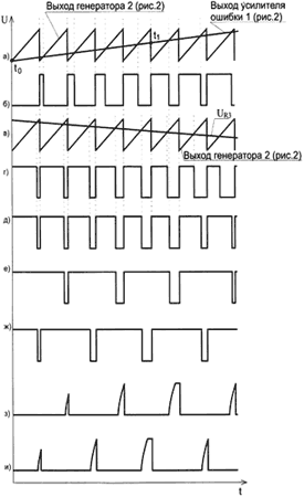
Fig. 3
Before each UPS on the capacitor C2 (Fig. 2), providing a smooth start, should be discharged. It's time to turn to the overall scheme of Fig. 1 voltage Converter. The function of soft start capacitor it performs the capacitor CP. When power is removed, the capacitor is quickly discharged through the resistor R1, the junction between the base and collector of transistor VT1 and diode VD1. Transistors VT1, VT2 function trigger protection. When applying an enabling voltage to the base of transistor VT2 it opens. Simultaneously opens the transistor VT1, continue capacitor NW and blocking, thus, the operation of the Converter voltage. The voltage from the collector of transistor VT1 through the chain R4VD2 holds open the transistor VT2. Disable trigger protection occurs only after removal of the voltage. As the power of the keys is equipped with a high field-effect transistors with a fairly large capacity gate-source. Therefore, to control these transistors used two sets of keys transistors VT3, VT5, VT7 and VT4, VT6, VT8.
Consider the work of one of them. When at pin 8 of the chip DAI high voltage is present (transistor inside the chip is closed), open field-effect transistors VT3 and VT7. Last bypasses the gate capacitance of the transistor VT9, instantly discharging it. The transistor VT5 is closed. Once at pin 8 of the chip will be set low voltage, transistors VT3 and VT7 closes and VT5 will open and the gate of the transistor VT9 will go gate trigger voltage. Resistor R18 prevents the failure of the transistors VT5, VT7, if one of them is closed, and the other is not fully opened.
Waveforms of the gate voltages of transistors VT9,VT10 shown in Fig. 3,3, I. In the circuit of transistor gates VT9, VT10 included resistors R20, R21, together with the capacitances of the gates form a lowpass filter that reduces the level of harmonics when the lid of the keys. Circuit R22, R23, C8, C9, VD5-VD8 also serve to reduce the harmonics of the inverter operation. The primary winding of the transformer T1 is included in the stock circuit transistor VT9, VT10. The feedback voltage to stabilize the voltage Converter is removed from the winding III of the transformer. Through the divider resistors R7, R8, it enters the chip DA1. Resistor R10 can slightly adjust the output voltage of the UPS. Elements R6, C4 determine the frequency of operation of the internal sawtooth generator circuits DA1 (if indicated in the diagram the values of this frequency is close to 50 kHz).
By changing the resistance of the resistor R6 and the capacitor C4, you can optionally change the frequency of operation of the Converter voltage. Power part of the circuit is powered via a mains filter C10, Cl1, L1, выпрямительVD4 and capacitors C12, C13. Resistor R24 discharges the filter capacitor in a switched-off transmitter. DA1 chip and keys transistors VT3-VT8 are supplied from a stabilized power supply on the elements T2, VD3, C5-C7 and stabilizer DA2. Resistor R25 is used to reduce the inrush current through the filter capacitor at the moment of start-UPS in the network. The rectifier output voltage of the Converter is implemented in a bridge circuit diodes VD12-VD15.
Soft start voltage Converter allows you to use in the secondary circuit capacitors filters quite a large capacity which is necessary for the power amplifier. Inductors L2, L3 together with the filter capacitors smooth out the ripple of the output voltage of the UPS. Protection voltage Converter flow transistors VT11, VT12. If you increase the current through the resistors R27-R30 transistors VT11, VT12 open and light up the LEDs in the opto-couplers Ul.l, U1.2. The transistor optocouplers are opened and fed to the base of transistor VT2 gate trigger voltage, which leads to trigger protection. Capacitor C1 prevents tripping of protection from random impulse noise.
Design and detailsStructurally UPS performed on a single-sided PCB (Fig. 4A, b).
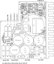
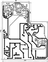
Fig. 4 a,b (click to enlarge)
The Board consists of all elements of the scheme, except SA1, FU1 and T2. Also on a separate small fee handed down resistors R22, R23 and capacitors C8, C9. They are connected by wires to the main Board at the points indicated by the letters a, b, C, Resistors R22, R23 strongly heated during operation, therefore, the fee should be positioned so that the resistors are not heated other circuit elements. Diodes VD12-VD15 are fixed on a separate needle radiator 10x12 cm and connect to the main Board wire diameter not less than 1 mm on one side of the PCB is the radiator (Fig. 4,6) with a length of 170 cm and a height of 10 cm.
It is desirable to use a needle radiator, but at least come any other. This radiator through the insulating strip is attached elements DA2 Board, VD4, VT9, VT10. On the opposite side of the radiator install the fan so that the flow of air blew the radiator. You can use a fan from a computer power supply. Food it is fed through resistor 320 Ohms and a power of 7.5 W output +50 In the transmitter. You can use a resistor type sew and clip it anywhere on the body. It is also possible to power the fan to wind an extra winding in the transformer T1 (Fig. 1). For this you will need to wrap two turns of wire with a diameter of 0.4 mm and connect the fan according to Fig. 5.
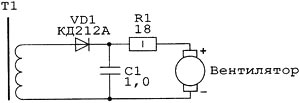
Fig. 5
The Converter transformer T1 is wound on four stacked rings of ferrite 2000NM sizes CHH. Coil transformer data given in the table.
Winding Number of turns The wire diameter, mm I and II 32 1,2 III 2 0,4 IV and V 7 2,4 (two wire 1.2 mm)The windings I and II of the transformer windings is separated from the group two or three layers of varnished cloth. The transformer T2 use ready with a variable voltage of 16 V. the Coil L1 consists of 2x20 turns, wound on a ferrite ring ferrite 2000NM sizes Ksh in the two wires with a diameter of 1 mm. Coil L2, L3 is wound on the ferrite pieces with a diameter of 8…10 mm and a length of about 25 mm wire diameter of 1.2 mm in a single layer along the entire length of the ferrite. In the Converter circuit, it is desirable to use imported electrolytic capacitors nous 105°. In the extreme case, the permissible use of other capacitors of appropriate size. The capacitor C12 recruited from three capacitors 220 V. mcfh
Nonelectrolytic capacitors of any type, for example K73-17. As the resistor R25 used three parallel resistor type SCK105 or similar, used in computer power supplies. Resistors R22, R23 C5-5-10W, R27-R30 - C5-16V-5W. The remaining resistors of any type, such as MLT. Trimmer resistor R9 type SPZ-AV or other small-sized. High frequency diodes, it is desirable to use, as shown in diagram (CD and CD), as imported diodes, now widely common, doesn't always work well at high frequencies, especially above 50 kHz.
Diode bridges can apply any appropriate size: VD3 - with rectified current of at least 500 mA; VD4 - with rectified current of at least 8 and a voltage of not less than 400 V. the Transistors BSS88 can be replaced by other similar field-effect transistors with insulated gate and an n-channel (the voltage of the source-drain of more than 50 V, the drain current of 0.15…0.5 A). This can be a types of transistors part no bss123, BS108, 2SK1336, etc., Instead of powerful field-effect transistors 2SK956 suitable types of transistors 2SK787, IRFPE50. Chip TL494CN can be replaced by chip TL494LN that will allow you to use a voltage Converter when ambient temperatures down to -25°C, as TL494CN functional only when the temperature is above 0°C. Also it is possible to apply the analog CAV. The optocoupler ABS can be replaced AUTOS, PS2501-2. As a chip DA2 can be applied CREE or 7815. In the case of using the IC 7815 in insulated casing when installing it on the radiator insulating spacer is not required. Transistors CTE, CTE permissible to replace CTG, CTG, and diodes KDE - almost any pulsed diodes, for example, CD, KD522, etc.
Setting
Before switching on the inverter in the network need to remove the supply voltage from the power circuit and apply power only to the transformer T2. First make sure that the power supply voltage +15 V output DA2. Then use the oscilloscope is satisfied pulses at the gates of field-effect transistors VT9, VT10 and their waveforms Fig.H.W, I. When the circuit is shorted capacitor NW pulses should disappear, and the gates VT9, VT10 be set to zero voltage. Next, by setting the slider of the resistor R9 to the middle position, serves the power supply for the rest of the circuit.
Use a voltmeter to monitor the voltage at pin 1 DA1, setting a value of 2.5 In the selection of the resistance of the resistor R7. A trimming resistor R9 is possible to a small extent to vary the output voltage of the Converter, however, you need to monitor the pulses at the gates of field-effect transistors VT9, VT10, their duration did not approach the extreme limits (too short or too long), and was in the middle position. Otherwise, when an increase in load or a change in supply voltage, the output voltage regulation will be impaired.
In order not to overload the voltage Converter and burn powerful field-effect transistors, the protection setting current is better to perform the following way. Temporarily solder instead of resistors R27-R30 resistors resistance of 1 Ohm and a power of 2 watts. To output connect the load and the ammeter. Set the load current to 1.3… 1.4 A and the selection of the resistances of the resistors R32, R33 achieve actuation current protection. Then solder the resistors R27-R30. In this configuration the voltage Converter can be considered finished. If the amplifier or any other load requires a different voltage, the output voltage of the Converter can be changed by changing the number of turns of the windings IV and V of the transformer T1. It should be borne in mind that in a single turn secondary winding is about 7 V.
According to the magazine, glad I oamator; Publication: www.cxem.net