


")

The described power unit is intended for use in Amateur radio lab. Although in Amateur literature was printed a number of schemes such devices, this power unit is not demanding to specialized chips and imported elements. Currently, the acquisition of the chips are still relevant and in some regions, to get them problematic. This power unit is an upgrade of the power supply unit described in ( II ). The power supply is built only from available parts.
Specifications power supply:
The output voltage is adjustable from 0 to 30 V.
The output current of 5 A.
The voltage drop at a current of 1 A to 6 A is negligible and at the output indicators are not reflected.
The diagram of the power supply shown in Fig. 1 below
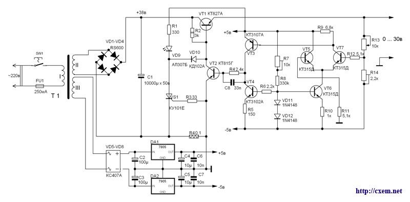
Fig. 1
This power supply consists of three major units: the internal network node power VD 1 - VD 4, C 1 - C 7, DA 1, DA 2, the node overload protection and short circuit VS 1, R 1 - R 4, VD 3 and the primary site - adjustable voltage regulator VT 2 - VT 7, VD 4 - 5 VD, R 4 - R 14, C 8.
And as to the power unit is added digital panel, i.e. the indication unit, which is shown in Fig. 5.
Internal network node power built in the traditional network transformer T1.
Node protection features has not. The current sensor was calculated for a current of 3A, but it is possible to calculate and 5A. For a long time the power supply was operated with a current of 5A. No malfunction was observed. Diode HL 1 indicates over-current or short circuit in the load.
The primary site - adjustable voltage regulator compensation type. It contains the input differential stage transistors VT 5, VT 7, two stages of amplification transistors 3 and VT VT 2, and the control transistor VT 1. Elements VT 4, VT 6, VD 4, 5 VD, R 5 - R 8, R 10 form stabilizers current. Capacitor C8 prevents the excitation unit. Because VT transistors 5 and VT (7) were not getting the same then there is a certain "zero offset" of the cascade, which is the minimum voltage of the power supply. The small range it is controlled by tuning resistor R 7 and, in the author's version reached at the output of the power supply is approximately 47 m V . Output voltage is adjustable resistor R 13. The upper limit voltage - trimming resistor R 14.
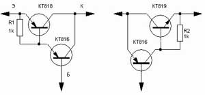
Fig. 2
Transistor CTA - composite. It can be replaced by a pair of transistors, as shown in figure 2.
These transistors connected to the Darlington circuit. Resistor R 4 is selected empirically, over-current protection operation. Resistors R 7 and R 14 - multi-SP5-2. Resistor - R 13 any variable with a linear functional response (A). In the author's version of the applied variable resistor PPB-3A 2.2 To - 5% . Chip DA 1 and DA 2 can be replaced with similar domestic CREA and CREA. Their power allows the stabilized voltage of ± 5 V to power external loads with currents up to 1A. This load is a digital panel that is used for digital display of voltage and current in the power supply. If you do not use a digital panel, chip DA 1 and DA 2 can be replaced by circuits 78 L and 79 05 L 05.
Printed circuit Board power supply unit shown in Fig. 3 and Fig. 4.
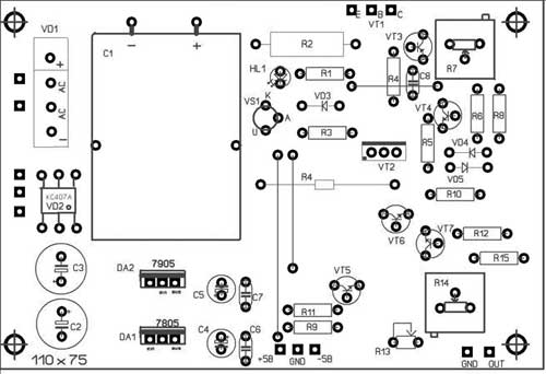
Fig. 3
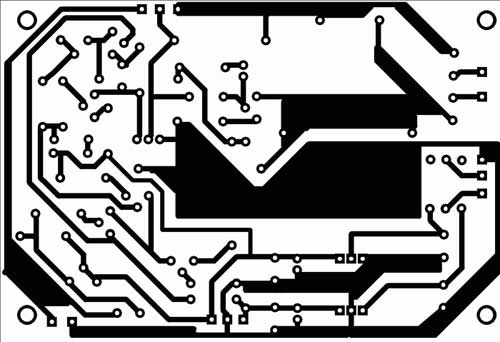
Fig. 4
Establishing
Since the structure is on two printed circuit boards, first configure the PSU, then the block of the digital display.
The PSU. With proper detail and the absence of errors in mounting the device begins to work immediately after turning on. Its establishment is to establish the necessary limits of variation of the output voltage and current protection. Engines resistors R 7 and R 13 should be in the middle position. Resistor R 14 to achieve a voltmeter readings 15 volts. Then the engine of the resistor R 13 is transferred to the minimum position and the voltmeter resistor R 7 set to 0 volts. Now the engine resistor R 13 is transferred to the maximum position and the resistor R 14 on the voltmeter set voltage of 30 volts. The resistor R 14 can be replaced by a constant, this Board has in place the resistor R 15. In the author's version is a resistor 360 Ohm. PCB size power supply 110 x 75 mm . Diodes VD 3 - VD 5 can be replaced by diodes CDB.
Digital panel consists of the input voltage divider and current, IC CREW and display of four seven-segment LEDs, shown in figure 5. Resistor R 4 digital panel consists of two pieces of wire wire ? =1 mm and a length of 50mm. The difference in the value of the resistor should not exceed 15 - 20%. Resistors R 2 and R 6 brand SP5-2 and SP5-VA. The mode switch indication of voltage and current type P2K. Chip KRUA is a Converter 3.5 decimal places, working on the principle of sequential accounts with double integration, with automatic zero point correction and polarity of the input signal.
For indication was used imported led seven-segment indicators KINGBRIGT DA 56 - 11 SRWA with a common anode. Capacitors C2 - C4 desirable to use a film type K73-17. Instead of import seven-segment LEDs can be used with domestic common anode type ALSB.
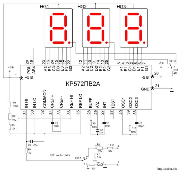
Fig. 5
Digital panel display of voltage and current
After power up and error-free installation, with proper parts must be lighted in the display segments HG 1 HG 3. The voltmeter resistor R 2 on the leg 36 of the chip CRP exhibited a voltage of 1 volt. To the legs (a) and ( b ) connect the power adapter. At the output of the power supply set voltage 5 … 15 volts and choose the resistor R 10 (roughly), replacing it for a time, alternating. Resistor R8 establish a more accurate indication of the voltage. Then, to the output of the power supply unit is connected to a variable resistor power 10 … 30 watt, put on the ammeter, the current is 1A and the resistor R 6 put the value on the indicator. The reading must be 1,00. At a current of 500 mA - 0,50, at a current of 50mA of 0.05. Thus, the indicator may indicate the current from 10mA, ie 0,01. Maximum readout current 9,99 A.
For higher resolution display it is possible to apply the scheme on CREW. PCB size digital panel 80 x 50 mm. Fig. 6 and Fig. 7. Contact pads U and I on a printed circuit Board digital panel, with the flexible wires are connected to the points corresponding indicators 2 and HG HG 1. Chip CREW can be replaced with imported chip ICL7107CPL.
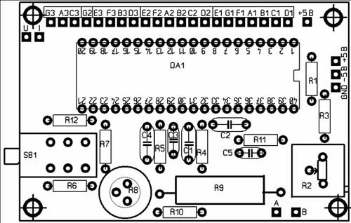
Fig. 6
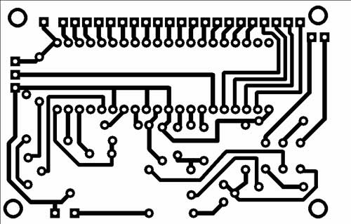
Fig. 7
Literature
Stable rectifier type TPP 12
- 3 - NT. g Gorce Delchev. Bulgaria. 1984.
A. Patrin Laboratory power supply 0…30 V. RADIO No. 10 of 2004. p.31.
The switching power supply based PCs. C. Mitiurev. RADIO No. 10, 2004. p. 33.
A. Anufriev AC cord ing for a home lab. Radio, 1992, No. 5, P. 39-40.
* Voltage regulator with double protection, Y. KURBAKOV, RADIO February 2004. p. 39.
S. Biryukov Handheld digital multimeter. - To assist radio Amateurs, vol. 100 - DOSAAF, 1988. p. 71-90.
S. Biryukov Digital devices in MOS integrated circuits. - M.: Radio and communication, 1990:1996 (second edition).
Radio N 8, 1998. p. 61-65
Author: Digital Voltmeter; Publication: www.cxem.net