


")

In the repair line scan TV quite often faced with the need to check the output transformer, deflection coils, and attached chains to them. But since horizontal scanning (main energy consumer in the TV) is working closely with power supply and nodes of protection, in violation of her protective device is triggered and test it the work is difficult. Sometimes, immediately after turning on the TV, instantly fail powerful (so-called power transistors are lowercase sweep or power source. In such apparatus generally cannot be checked the output stage and its elements by conventional methods.
In these cases it is recommended to use simple method test line scanning, using a simple device-tester. Check only the output stage when the TV is turned off. The device allows to determine faulty if the cascade, and to identify the defects of the output transformer and deflecting coils.
When checking with a tester on the output stage receives the supply voltage 15 V, which changes the voltage of 120..140 B, and the pulses with a repetition rate of about 15625 Hz. They simulate operation of the output transistor. Therefore, the check is performed at reduced voltage that does not interfere to control the oscilloscope and measuring the current of the main parameters of the cascade.
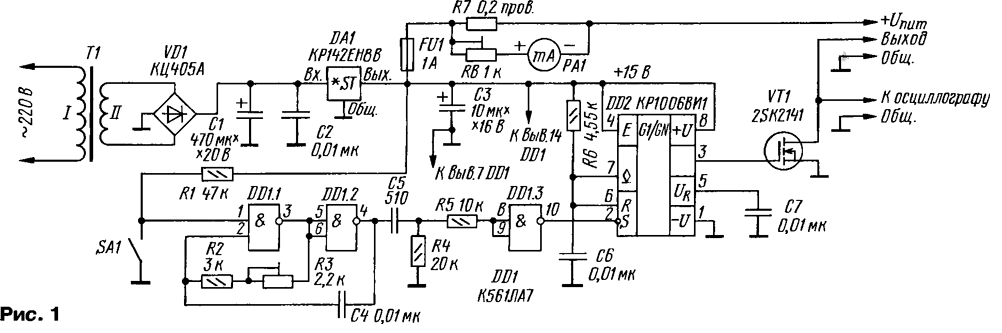
A schematic diagram of one of possible variants of the tester shown in Fig. 1.
(click to enlarge)
It consists of a voltage source of 15 V and a generator of pulses about 50 μs with a specified repetition rate. Using the key on powerful field transistor VT1 pulses serves to output flyback transformer by the circuit Fig. 2.
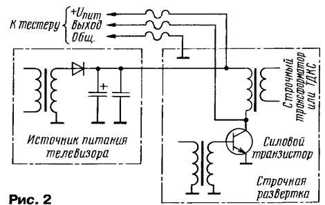
The pulse generator (see Fig. 1) built on chips DD1 and DD2. Actually the generator is assembled on the elements DD1.1, DD1.2. Its work if necessary to lock the switch SA1, connects pin 1 of the element DD1.1 General wire. As a result of the passage of the pulse generator through the differentiating chain C5R4 at the exit of the element DD1.3 are obtained with short pulses, triggering the single vibrator DD2. He, in turn, produces output pulses duration of about 50 microseconds. And since the repetition rate of short pulses equal to 15625 Hz , the duration of the pauses between the output pulses reaches 14 ISS. They arrive at the gate field-effect transistor VT1, operating in key mode, and open it. The drain and source of the transistor VT1 is connected respectively to the collector and emitter of the output (power) transistor horizontal (see Fig. 2). And the transistor sweep if he is serviceable, no need to unsolder, as it does not interfere with the operation of the tester.
The device also includes (see Fig. 1) voltage stabilizer DA1 15 In, the output circuit of which includes a pointer (the author) measuring current RA1, consumption of output stage line scan. This stabilizer eat the chip tester.
Details of the device is placed on a circuit Board made of fiberglass (or dummy Board). It is placed in a small plastic case. On its exterior panels fix socket for connecting an oscilloscope and the device itself to lowercase scan. Pointer-type measuring current can not be applied (when not needed and resistors R7, R8), and to place on the outside of the tester slots connect one meter. The fuse FU1 is better to leave to protect the instrument.
Before connecting the tester to the TV, you need to check for short circuit the power circuit of the horizontal sweep (then you need to look for the defect in this chain) and between pins collector and its emitter of the output transistor. Repeat, what if the transistor is broken, it may be given. In the absence of transistor circuit leave in place.
The output stage line scan testing, measuring consumed current and controlling the oscilloscope form and duration of the flyback pulses, which occur at the drain of the FET VT1 during operation of the tester. Obviously, what with supply voltage 15 V, eight or nine times smaller real voltage, the amplitude of all measured pulses will be in the same number of times less than working in TV, but their shape will not change.
Current consumption should be in the range of 5 to 70…80 mA (depending from building line scan TV). If the consumption is less, in the output stage is broken. This can be either bad soldering, or cracks in the printed guide, or cliff primary winding of the flyback transformer (which is quite rare).
If the current exceeds 80 mA, in the cascade has a leak. It can be both direct or alternating current. To delimit the switch SA1 block generator. Thus the horizontal sweep circuit should consume DC 5… 10 mA. If it exceeds these values, check rectifier diode and filter capacitor of the power source, and fed the output transistor horizontal. If the current is still large, need to disable all the elements connected to the power circuit.
After the fault in the power circuits control the current when enabled the generator of the tester. It needs to be within the limits specified above. If he greater than 80 mA, the most likely cause of leakage AC may to be a breakdown voltage multiplier. There are also leaks in the secondary the circuits of the flyback transformer or the breakdown between the windings. In the import the TV in the first place you should check all the rectifier diodes and capacitors and secondary power supplies connected to stronomy the transformer TDKS, as well as to ensure that no short circuit in some of these circuits when disabling them one at a time. Very often the cause circuit becomes a protective Zener diode connected in parallel to the source power 12 V. the Fault TDKS not such a frequent phenomenon, and, most likely, leak detected in the secondary circuit.
If the power consumption is normal, the screen of the oscilloscope observe the impulses reverse. The shape and the obtained pulse duration of the show does the circuits of the flyback transformer and deflection coils need the timing and have hit a resonance. The pulse duration should be in the range of 11 to 16 microseconds. It is the reactive elements output stage: mainly by the inductance of the flyback transformer and deflecting coil, and the capacitance reverse and capacitor connected in series with the deflection coil. If the pulse duration is not correct, the fault're looking for in these circuits.
In the tester you can use any resistors and capacitors. The resistor R7, when the lack of industrial, made from a piece of nichrome wire with a diameter of 0,2-0,4 mm. Resistor R6 consists of two or three resistors connected consistently.
Diode bridge CCA you can replace individual diodes, for example, CDA, and chip CREW - CREE or LM7815. It must be hosted on a small heat sink, as in the process of testing a defective TV through the stabilizer can flow relatively large currents caused by leakage. DD1 chip similar interchangeable from C. But from C, only then you will need to add a stabilizer with the Zener voltage 10… 12 V Chip CREW can be replaced import analogue of the LM555. On the position of VT1 is possible to use transistors 2SK2038, 2SK792, CPD.
The transformer T1 can be any voltage at the secondary winding 16 of the 19th Century… The author has used transformer TPP connected in series with windings 11-12, 13-14, 15-16, 19-20. Microammeter RA1 - M2001 or similar with current full deflection of 50 μa.
The establishment of the tester is not difficult. It consists in setting the milliammeter RA1 and the necessary adjustment of the frequency and duration of the weekend pulse tester. For calibration of the scale of the milliammeter between nests "+IPIC" and "General." include a resistor of 30 Ohms and a trimming resistor R8 set the milliammeter reading 500 mA. If desired, the scale of the device you can mark the color labels 5 and 80 mA. Further connected to the pin 4 chip DD1 oscilloscope and a trimming resistor R3 controls the frequency pulse about 15625 Hz. After that, connect the oscilloscope to conclusion 3 chip DD2 and convinced of the presence of its rectangular pulses duration of about 50 microseconds. The slight deviation of the frequency and duration pulses from the above is irrelevant. If necessary the pulse duration can be changed, picking up the resistor R6 or a capacitor C6.
For more reliable operation of the generator on the elements of the DDI. 1, DD1.2 it is better to add another element DD1.4, which has remained free in chip. Turn it on, combining inputs, between the connection point of the output item DDI.2 and the capacitor C4 and the left (the scheme) of the output capacitor C5. To the connection point of the new DD element 1.4 and capacitor C5 is connected right (under the scheme) the output resistor R3, unplugging its findings 3, 5. 6 chip.
Author: I. Korotkov, p. Bucha, Kiev region, Ukraine