


")

In the package "PS one", except the system unit (console), enter joystick DUAL SHOCK, plug the AC adapter and cable to connect to TV. A demonstration CD is missing. Cable and joysticks all models "PlayStation" unified. Diagram located in the unit system and network processor boards adapter discussed below. This is not the official manufacturer's documents IIP, they - the result of the analysis of printed circuit boards multiple instances of the console. Positional designation of most of the elements are given in accordance with the marking on the PCB. To unfortunately, installed on the CPU Board chip resistors and ceramic chip capacitors not marked. Therefore the numbers in positional notation "brand" do not match. Rated power of chip resistors is defined by their sizes: 1206 - 0.25 W; 0805 - 0,125 W; 0603 and 0402 -0,063 watts.
PROCESSOR BOARD
The complete scheme of this main part of the top box divided roughly into are some. Fig. 1 contains nodes of the computing system TRS based 208-pin VLSI 1C 103 CXD8606CQ. In addition to a 32-bit RISC processor core, R3000A compatible with company MIPS, it contains the program memory (4 Kbytes), memory data (1 Kbyte), block General purpose registers, the graphics accelerator GTE (Graphic Transfer Engine), controllers, direct memory access, interrupts, external dynamic RAM and cache memory, three 16-bit counter-timer, two serial port I / o, JPEG decoder. Processor signal Tekirova CLK. In conclusion CPU 76 through a chain R25C115 signal RES setting the system in the initial state. Included in series in the circuit some conclusions VLSI low-resistance resistors are used to eliminate "ringing" on the swings pulses.
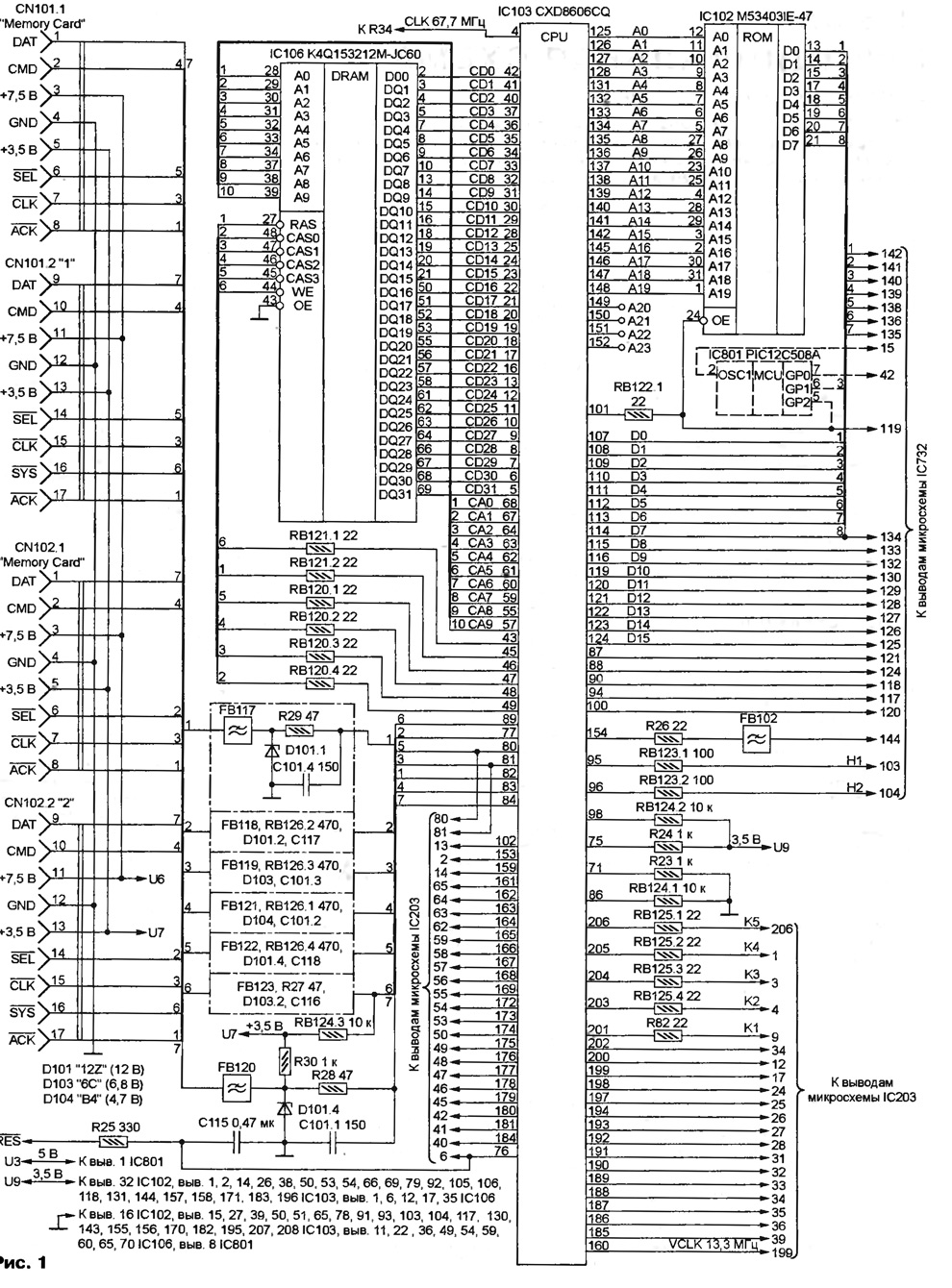
(click to enlarge)
High-speed 32-bit data bus CD0-CD31 and address bus CA0-CA CPU is associated with dynamic RAM IC106 K4Q153212M-JC60 volume 2 MB. Earlier this the chip was released under the name KM432V515.
The eight-bit mask ROM IC102 M53403IE-47 - custom. The last two digits (47) the name is the version number of the firmware ROM. In the official specifications parameters "PS one" appears with a volume of 512 Kbytes. However, the 20-bit bus addresses AO-A19 allows you to access twice the greater number of cells. ROM chips installed in two different 32-bit patterns "PlayStation", interchangeably. This circumstance use in the repair.
Connectors CN101.1, CN101.2, CN102.1, CN102.2 are designed to connect to TRS joysticks and memory cards. All of their input and output circuits are protected from interference and damage filters FB117-FB123, Zener diodes and their assemblies D101, D103, D104, as well as RC circuits.
The dashed lines in Fig. 1 shows a chip IC801 PIC12C508A. So called "mod-chip" microcontroller, programmed in such a way that runs CD's as a brand (with dark purple surface), and non-branded (silver surface) produced by different regional facilities. Place on the circuit Board that the chip is not provided, it is hinged connected by wires. As IC801 used the various microcontrollers series PIC, AT90S, Z86), often with erased the names and cut the "extra" pins. However, those that are intended for still variants "PlayStation", "PS one" are not suitable.
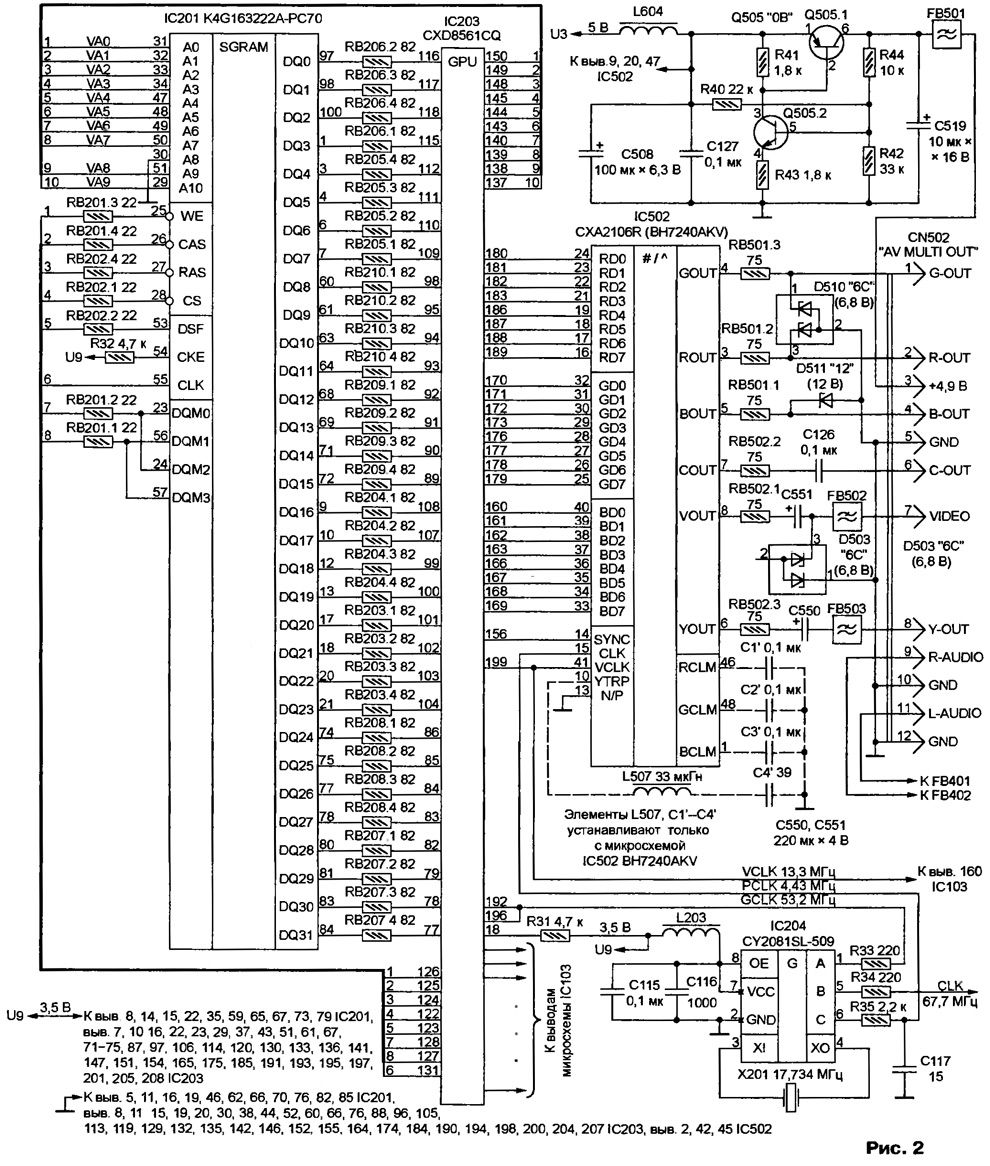
We turn now to Fig. 2. Shown here 208-pin GPU IC203 CXD8561CQ functionally equivalent to ZD accelerators, used in IBM PC graphics cards. He is responsible for drawing on the screen of polygons rotation and scaling of sprites, the shading of the contours of the Gouraud algorithm. Every second the processor can handle up to 360 thousand polygons. Total performance - 66 million operations per second. Resolution from 256x256 up to 640x512 pixels in the TV standard to PAL or from 256x240 to 640x480 pixels in NTSC. A large number of lines connects the graphics processor with CPU - chip IC103 (see Fig. 1).
(click to enlarge)
In conjunction with the controller IC203 works video RAM IC201 K4G163222A-PC70 - dynamic synchronous, with capacity of 16 Mbit. Doubled compared to installed in previous models the information capacity of the chip video RAM gave a reason to talk about the enhanced graphics "PS one". However, it is not. 11 address inputs AO - a10 chips only used ten, input A8 is connected a common wire. So active as before, only 8 MB of video memory.
If you suspect a faulty video RAM (image shows extra point or line), you can try to switch to "spare" half chip IC201, disabling the output 30 of the total wire and connecting it with one of the power pins chip.
From the outputs of the GPU IC203 eight-bit digital video signals primary colors are received at the inputs of RDO-RD7 (red), GD0 - GD7 (green) and BDO-BD7 (blue) chip IC502 CXA2106R, replacing two that were used in early models IWP: videocap and signal Converter RGB to full a television signal of PAL or NTSC.
Sometimes as IC502 chip installed BH7240AKV. Coinciding with CXA2106R on the main characteristics and purpose of most of the findings, it requires several additional elements shown in Fig. 2 dashed lines. Space the Board is designed for them.
Derived at the output connector CN502 chain of video signals is supplied with a matching resistors, protective Zener interference suppression filters. Voltage +4.9 V, entering the same through the node connector overcurrent protection transistor the Assembly Q505, designed to supply TV RF modulator. The maximum load current is 85 mA, residual voltage after the protection operation is not exceeds 5 mA.
Note has changed compared to previous models "PlayStation" the numbering of the pins on the connector CN502, although their relative positions and the appointment of remained the same.
Programmable clock signal generator IC204 CY2081SL-509 - custom. The ratio between the values of the frequency of its output signals and quartz resonator H define constants recorded by the manufacturer the chip in her "one-off" internal ROM. Index 509 in the designation generator - the order number under which it is programmed. Frequency signals shown in Fig. 2.
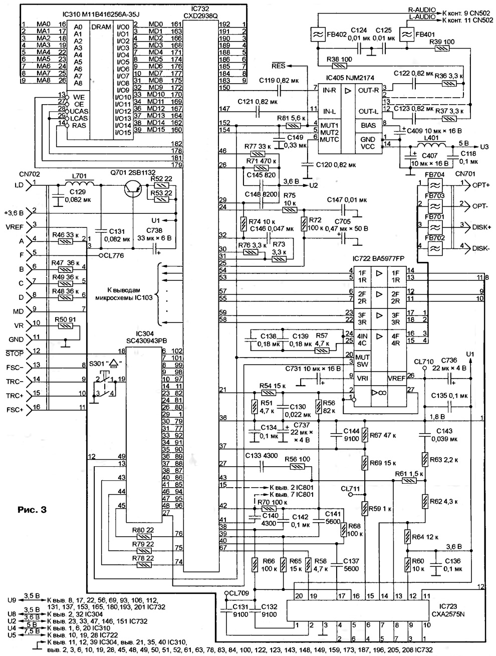
Part of the scheme the prefix "PS one", is depicted in Fig. 3, the system includes processing of audio and control data interface and CD-ROM. Compared to previous models, the system that processes digital data "PS one" significantly simplified, there were only two chips controller IC304 and SC430943PB 16-bit dynamic audios IC310 M11B416256A-35J capacity of 512 KB. However, functions have not diminished. The explanation is quite simple - decoder data CD, buffered static RAM, 256 Kbps, the data unpacker MPEG-1, audio processor, DAC and became part of the 208-pin VLSI IC732 CXD2938Q, formally belonging to the system interface CD-ROM. GSI operates under running CPU IC103 associated with many lines.
(click to enlarge)
Formed VLSI IC732 stereo sound arrives at dual channel amplifier IC405 NJM2174, and its outputs through the filter to the appropriate the contacts of the connector CN502. The amplifier operates only when a certain combination logic levels on the control inputs (pin 4 is high, pin 5 - low). This property is used to prevent playback distorted signals and noise during the installation of the nodes TRS to its original state and start programs.
Sometimes the amplifier NJM2174 substitute functional equivalents with additional electronic keys for lock outs.In NJM2174 such keys are not, they conclusions (2 and 13) is not involved, odnako running printed conductors (shown by dashed lines), the Board has always.
To the connectors CN701 and CN702 connect the CD-ROM drive KSM-440BAM, electrically compatible with used in previous models "PlayStation" ([2], Fig. 22), but with the connecting loop of a different size and configuration. The semiconductor laser the optical head actuator included in the collector circuit of the transistor Q701 2SB1132. Current laser adjust trimmer resistor in the drive. Indirectly this current can be measured by the voltage drop across the resistors R52, R53 (0,66 0,88… In correspond to 60…80 mA).
The signals from the photodetectors of the optical head arrives at the inputs of the chip IC723 CXA2575N that performs the functions of amplification, equalization and pre processing. Further processing takes place inside VLSI IC732. She generates the control signals to the electric motors and electromagnets of the actuator The CD-ROM supplied to the corresponding node through the power amplifier chip IC722 BA5977FP. Its analogs - BA5947FR AN8732SB. Established in the early models "PlayStation" chip BA6392FP, BA6397FR, BA6398FP differ from BA5977FP the pin assignment.
Button SB301 mechanically connected to the lock-chamber, in which is mounted the game disc. When it is open, the contacts are open.
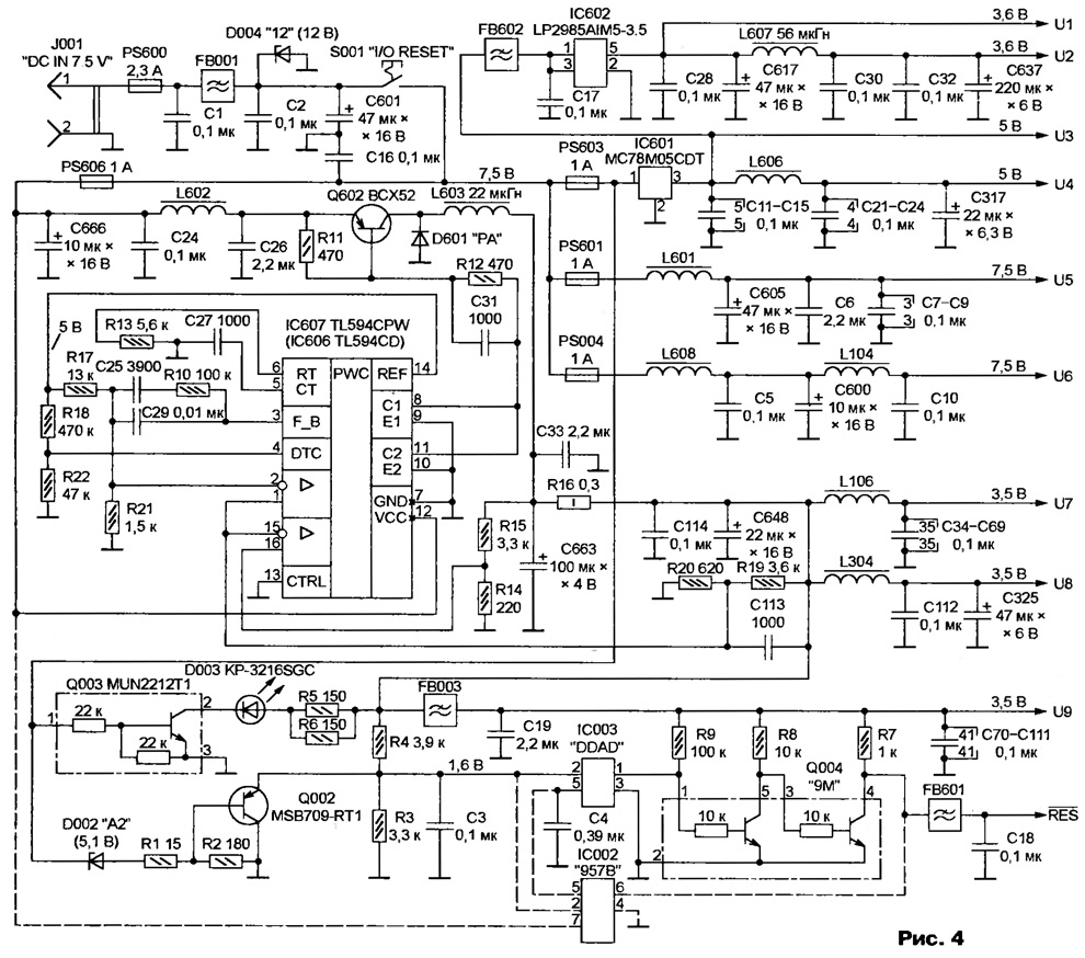
The system unit "PS one" nourish a constant voltage of 7.5 V from remote AC adapter - network adapter, the scheme which will be discussed in the next section. On the CPU Board from the voltage get all other necessary for the operation of its nodes. Diagram of circuit boards shown in Fig. 4.
(click to enlarge)
Voltage 7.5 V comes with connector J001 through the fuse-link PS600, filter FB001 and S001 push-button switch. From random feed connector 1001 too large or reverse polarity voltage processor Board protects Zener D004. Proceeding in these cases through the opened Zener diode is very high current leads to the burnout of the fuse PS600 or protection the network adapter.
Using fuse PS004, PS601-PS603 input supply voltage distribute among several consumer groups. Voltage in the circuits U1, U2 (3.6 V) and U3, U4 (5) stable linear integral stabilizers accordingly IC602 LP2985AIM5-3.5 and IC601 MC78M05CDT, and output the second voltage (5 V) is input to first.
In the circuit U5 and U6 serves voltage 7.5 V without additional stabilization. A voltage of 3.5 V in the circuit U7-U9 comes from a switching regulator, main whose elements are the key transistor Q602 WSH, damping diode D601, storage choke L603 and pulse width (SHEA) controller IC607 TL594CPW. It is similar to known TL494 (CREW), a brief description and principle of operation which can be found e.g. in [3].
Sometimes, instead IC607 on a designated place on the Board set chip IC606 TL594CD that differ only in case design. Resistor R16 serves as a sensor of the load current of the stabilizer.
All power circuits are provided LC-filters, smoothing oxide and interlocking ceramic capacitors. Just on the surface of the PCB fairly evenly distributed over hundreds of such capacitors.
The D003 led serves as an indicator of the inclusion of TRS. It glows in the presence of voltage 7.5 V after the fuse PS603 and 3.5 V on the output pulse stabilizer.
One of the differences of the "PS one" from the previous models is the lack of dedicated buttons RESET to install the system to its original state. Signal initial installation RES is generated automatically each time you turn the console switch S001 or after emergency short-term decline and recovery to nominal the value of the supply voltage of 7.5 V.
After power-up, the single vibrator IC003 generates on output 1 pulse low level, the duration of which (0,2…0,3) depends on the value of capacitor C4. The amplifier transistors of the Assembly Q004 brings to needed I needed power level momentum | through the filter which FB601C18 arrives at the inputs of the initial installation Mick-i roshem CPU Board.
If you reduce the input voltage below 6 closes In the Zener diode D002, and the transistor Q002 open, continue chain R3C3. The single vibrator IC003 sees a sharp decrease in voltage on output 2 off power, and after the restoration in the chain 7.5 V nominal voltage and closing of the transistor Q002 generates a pulse initial setup.
In some instances, the processor Board driver signal RES is chip Q002, for which space is provided. In this case IC003 chip and some other related items are not set.
NETWORK ADAPTER
Remote power supply unit ASU "PS one", usually called a network adapter, unusually lightweight (180 g) and thin. Its size 57x88x30 mm. it has no usual step-down transformer at a frequency of 50 Hz, as applied high frequency the voltage Converter with an efficiency of 70…78%. Nominal output voltage is 7.5 ( Actually - 7.7 In, obviously, to compensate the voltage drop on the resistance of the wires connecting cord 1.8 m length). Voltage changes only 0.3% at load currents up to 2 a, And at 2.8 A is triggered overload protection. The amplitude of pulsations - 20…60 mV. Note that the adapters Japanese and American models "PS one" are not suitable for use in countries The CIS, as calculated on a different mains voltage.
The design of the adapter SCPH-114, manufactured in China under license of the firm SCEI, shown in Fig. 5. Please note, many circuit elements (resistors and capacitors) composed of several connected in series or parallel. In some cases this is done not to exceed power or voltage, in others for the exact setting required resistance. Positional notation elements in each of these groups different alphabetic index, with the same sequence number. In the links to group items by text indexes, as a rule, omitted.
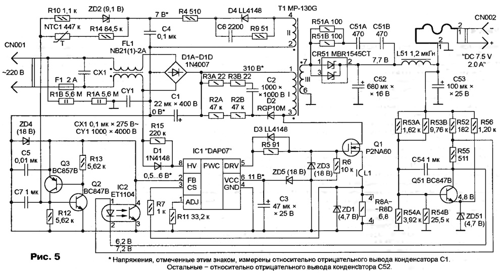
(click to enlarge)
Since the switch in the adapter is absent, the latter works all the time built-in plug CN001 inserted into the wall outlet, it is possible prolonged absence of load. The input circuit is protected against overload by melting insert F1 and LC noise filter CX1FL1. Unconventional position signs are given to the capacitors CH and CY1 to emphasize their special design. These capacitors are specially designed to suppress pulse and high frequency noise. The resistor R1 equalizes the potentials of the wires network and common wire TRS, preventing the accumulation of static charge.
Rectified by a diode bridge D1A-D1D and smoothed by the capacitor C1 voltage nourish single-ended flyback inverter FET Q1 and the transformer T1. Chain D2R2R3C2-damping. Voltage winding III transformer, rectified Assembly diodes Schottky CR51, appear on the output adapter connector (CN002). Chain R51C51 suppresses the reverse voltage surge on diodes. The capacitor C52 and the filter L51C53 decrease pulsation.
The output voltage of adapter is stable pulse width method. Control pulses of amplitude 10… 11 V and a frequency of 60 kHz received on the bolt transistor Q1 from the output of the CHI-controller IC1. The duty cycle depends on the collector current of the phototransistor of the optocoupler IC2 in the circuit output 2 CHI-controller. The current depends on the ambient light, creating a radiant diode OPTRON included in the output circuit of the amplifier of the error signal on the transistor Yes no total: Q51. The error signal is the difference of the output voltage of the adapter, remove from resistive divider R53R54, and exemplary taken with the Zener diode ZD51. Thus closes the circuit of the stabilizing feedback.
Mounted in the adapter SHIH-controller - analog NCP1200 chip firm "ON Semiconductor". It is made according to the technology, allowing to place one crystal chain both low and high (up to 450 V) voltage. Pulsating with 50 Hz unipolar voltage amplitude of 300 V is supplied to pin 8 of IC1 through the diode D1. Inside the chip (between pins 8 and 6) there is a kind of "damping resistor" is switched with a frequency of approximately 50 kHz source current 2.. .4 mA FET. This current charges is connected to pin 6 the capacitor C3 until the voltage is approximately 11V, which feed on low-voltage nodes of the chip. The voltage is kept within acceptable limits when the input variable in the range of 100 to 380 V. power dissipation "resistor" power does not exceed 0.25 W.
Diode D1 is a low voltage. During normal operation, the attached return the voltage does not exceed 0.7 V is the voltage drop across one of the diodes of the bridge D1A-D1D. However, the asynchronous switching of the internal power supply to supply network sometimes leads to a transient invalid voltage on the diode. This phenomenon eliminates the resistor R15.
On input 3 CHI-controller IC1 receives the signal of the current sensor is a resistor R8 in the circuit the source of transistor Q1. When the adapter without the load of SHI-controller goes in the mode with a reduced pulse repetition frequency, facilitating mode transistor Q1 and reducing consumption from the mains power. When the overcurrent generation becomes discontinuous. Short tutu control pulses are repeated every Of 0.7 C.
Transistors Q2 and Q3 connected in a analogue thyristor. Until the voltage on the output of the auxiliary rectifier (winding II of the transformer T1, the diode D4 and the capacitor C4) is less than the voltage stabilizing Zener diode ZD2, both transistors closed. In the case of increasing the mains voltage 40…50 % proportion increasing the voltage on the capacitor C4 and Zener diode ZD2 is opened. Current, the current through the resistor R10, opens "thyristor" Q2Q3, which bypasses the chain output 2 CHI-controller IC1, barring the latter's work and the adapter as a whole. Automatic return to operation mode in this case. Plug CN001 must be removed from the socket and re-paste.
The thermistor NTC1 is the security element. When the adapter overheating it the resistance is reduced, which should lead to the opening of the "thyristor" and Q2Q3 the block CHI-controller IC1. But in practice, the protection does not work, even if to close the findings of the thermistor. Caused by too large a value of the resistor R14, which should be reduced to 10 ohms.
Literature
- Ryumik S. "PlayStation": the History of development. Radio, 2002, No. 11, pp. 21 - 23.
- Ryumik S. "Sony PlayStation" or particular circuitry 32 bit video attachments. Radio, 1999, vol. 7, pp. 26-28.
- Alexandria R. Circuitry power supplies of personal computers. Radio, 2002, No. 6, pp. 22-24.
Author: S. Ryumik, Chernigov, Ukraine