


")

For charging storage batteries motorists use the a variety of devices, most of which are built using step-down power transformer. Such devices relatively peculiar low efficiency, large size and weight. And if the efficiency can somehow raise, to improve other indicators of such devices is practically not possible. Significantly improve the performance of battery chargers can, if to be built on the basis of the pulse voltage inverter.
Pulse charging stations, manufactured abroad (Bosch, Telwin, etc.), have excellent technical performance, but at a cost not available most of our motorists. Along with this, and independent production such devices do not each radio enthusiast, especially those who not have the necessary experience in the field of pulsed circuitry and establishing such devices.
However, it should not be assumed pulse chargers irresistible complex. Thus, in [1] described a ham radio device, based on flyback Converter.
The undoubted advantage of such converters is their relative simplicity and small dimensions. However there are some drawbacks. One of the most serious of them is the magnetization of the magnetic circuit of the transformer, because of what has to use the magnetic circuit section 2…2.5 times larger than for two-stroke transducers.
In addition, the emission voltage of the switching element flyback converters usually considerably higher than the power supply voltage that requires the introduction of further suppressing and heat recovery circuits. Energy losses in these, the most noticeable impact at high output power, therefore, single-ended converters are used in the power supply units capacity not exceeding hundreds of watts.
The battery of lead-acid batteries are usually charged in one of three ways: with stable voltage and stable current and on the so-called rule ampere-hours. The charging voltage is quite simple to implement, but it does not guarantee one hundred percent use of the battery capacity. Charging rule ampere-hours (Woodbridge) can be considered as the ideal way, but it is not widespread due to circuit complexity.
Recognized as the most optimal way to charge a stable charging current. The device for implementing this method to easily upgrade your units, which help to automate the charging process. This group of chargers applies described below.
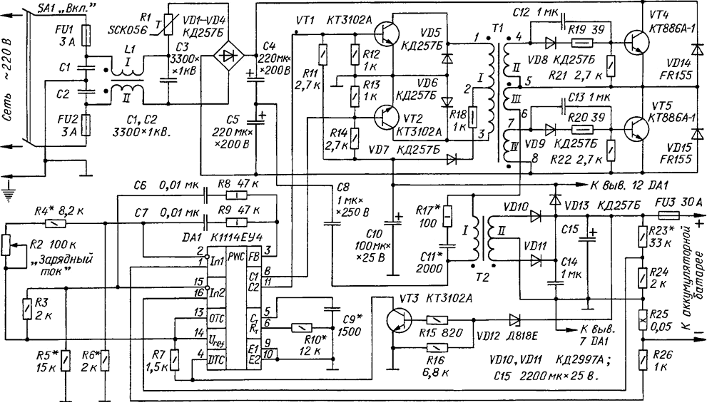
The basis of the device (see diagram) based on half-bridge push-pull pulse Converter (inverter) on a powerful transistors VT4 and VT5, managed generating a PWM controller DA1 the low-voltage side. Such converters, sustainable increase of the supply voltage and the change the load resistance, are well established in power supplies modern computers. Because the SHI controller KEU [2] there are two the error amplifier, to control the charging current and output voltage you want extra chips.
(click to enlarge)
High-speed diodes VD14, VD15 protect the collector junction transistors VT4, VT5 from reverse voltage on the winding I of the transformer T2 and discharged energy emissions back into the power source. The diodes should have a minimum switching time.
The thermistor R1 limits the current to charge the capacitors C4 and C5 when you turn devices in the network. To suppress interference at the transmitter side is mains filter C1C2C3L1. Chain R19R21C12VD8 and serve to R20R22C13VD9 forcing closing process of switching transistors by feeding in their basic circuit negative voltage. This reduces switching losses and to increase the efficiency of the Converter.
Capacitor C8 prevents Pogranichnyi of the magnetic circuit of the transformer T2 due to the varying capacitance of the capacitors C4 and C5. The chain contributes R17C11 decrease of the amplitude of surges on the winding I of the transformer T2.
The transformer T1 is electrically decouple the secondary circuit from the network and transmits the control pulses to the base circuit of the switching transistors. Winding III provides a proportional current control. The use of transformer interchanges allowed to make the device safe.
The rectifier charging current diodes made on CDA (VD10, VD11) capable to operate at relatively high operating frequency of the Converter.
Resistor R25 - current sensor. The voltage of the resistor, filed on the non-inverting input of the first error amplifier controller DA1, compared with the voltage at its inverting input, set by the resistor R2 "Charger current". When modifying the error signal varies the duty cycle of the control pulses, the open state of the switching transistors of the inverter and, therefore, transmitted to the load power.
The voltage divider R23R24, is proportional to the voltage of a rechargeable battery, is supplied to the non-inverting input of the second error amplifier and compared with the voltage across the resistor R5 is applied to the inverting input of this amplifier. Thus the regulation of the output voltage. This allows vigorous boiling of the electrolyte at the end of charging by reducing charging current.
SHEA controller incorporates a stable source of 5 V, which nourishes all voltage dividers, specify the desired values of output voltage the device and the charging current.
Since the power to the chip DA1 receives the output of the device is unacceptable the decrease of the output voltage of the device up to 8 In - in this case stops stabilization of the charging current and it may exceed the limit value. This situation eliminates the site, assembled on the transistor VT3 and the Zener diode VD12, - it blocks the incorporation of the charger, if its loading faulty or discharged battery (with EMF In less than 9). Zener diode, and hence, the transistor node remain closed, and the entrance DTC (pin 4) of the chip DA1 is connected through a resistor R7 to the output Uref source built reference voltage (pin 14). The input voltage DTC not less than 3 In, and the generation of pulses is prohibited.
When connected to the outlet of the device is defective, the battery offers a Zener diode VD12 and after him the transistor VT3, closing on a common wire input DTC controller and thus allowing the generation of pulses at the outputs C1, C2 (outdoor the collector). The pulse frequency is about 60 kHz. After amplification of the current transistors VT1, VT2 they through the transformer T1 is transferred to the base switching transistors VT4 and VT5. The pulse repetition frequency is determined elements R10 and R9. It is calculated by the formula F=1,1/R10·C9.
Diodes CDB can be replaced by RL205, CDA - other, including diodes The Schottky reverse voltage of 50 V and the rectified current of 20 A, FR155 - for high-speed switching diodes FR205, FR305 and UF4005. SHI the controller KEY has many foreign counterparts - part no tl494in [3], DBL494, GLRS, IR2M02, CA. Instead CTA-1 suitable transistors CTA, or CTB CTB-1.
Transformers are the most important and time-consuming elements of any pulse the Converter. The quality of their production depends not only features devices, but in General its performance
The transformer T1 is wound on an annular magnetic core size of CHH ferrite MNM. Winding I wound wire sew-2 0,4 evenly throughout the ring and contains 2x28 of turns; winding II and IV - 9 turns of wire sew-2 to 0.5. III winding of two turns of wire MGTF and 0.8. The windings are insulated from one another and from the magnetic core with two layers of thin PTFE tape.
The transformer T2 is wound on an armored magnetic Sh ferrite MNM (or, even better, M2500HMC); suitable annular magnetic core similar section. Winding I contains 35 turns of wire sew-2 0,8 and winding II - 2x4 revolution harness with not less than 4 mm2 several wires sew-2 or PEL. If forcibly cooling the transformer, the cross section of the wiring can be reduced.
It should be noted that the quality of the winding insulation of transformers depends not only the reliability of the device, but also the safety of its operation, as it isolates the secondary circuit from the line voltage. Therefore it is not necessary to execute it from scrap materials - wrapping paper, stationery tape and etc. - and even more so to neglect her how sometimes make inexperienced ham radio operators. It is best to apply a thin Teflon tape or condenser paper from the high voltage capacitors, putting it in 2-3 layers.
Assemble the device in a metal box of suitable size. Transistors VT4 and VT5 is mounted on the heat sinks with a surface area of at least 100 cm2. Diodes VD10, VD11 also provide a common heat sink with a surface area of not less than 200 cm2. To use as a heat sink wall box device, and also a common heat sink for the diodes and transistors should not be reasons safety of the battery charger. The sizes of sinks can significantly reduce, if forced to cool them with a fan.
To establish the Converter will need Latr, oscilloscope, serviceable battery and two meter - voltmeter and ammeter (up to 20 A). If there is a ham radio operator will be an isolation transformer 220 x 220 V power not less than 300 W, the device should be enabled by using it to work would be safer.
First, through the temporary current limiting resistor of 1 Ohm capacity of not less than 75 watts (or car lamp with a capacity of 40-60 watts) connect to the output device the battery and assured that there is a positive voltage of 5 V on the output Uret (pin 14) CHI controller. Connect the oscilloscope to the outputs C1 and C2 (findings 8 and 11) of the controller and see the control pulses. The engine of the resistor R2 set in the lowermost according to the scheme of position (minimum charging current) and served from Latri on mains input voltage 36.. .48 V. Transistors VT4 and VT5't get too hot. The oscilloscope control voltage between the emitter and the collector of these transistors. In the presence of emission at the front pulses should be applied more high-speed diodes VD14, VD15 or more precisely pick up the items C11 R17 and the snubber circuit.
You must keep in mind that not all oscilloscopes allow measurements in the circuits are galvanically connected to the network. In addition, remember that part components of the device is the AC line voltage is unsafe!
If everything is OK, the voltage at the network entrance gradually increase Latri to 220 In and control the operation of transistors VT4, VT5 on the oscilloscope. Output current this must not exceed 3 A. Rotating engine of the resistor R2, one can see in a smooth the change of the current output device.
Further, from the output circuit delete this temporary current limiting resistor (or the lamp) and connect the battery directly to the output device. Choose resistors R4, R6 to change limits the charging current regulator R2 were equal to 0.5 and 25 A. Set the maximum output voltage is equal to 15V selection of resistor R5.
The handle of the regulator R2 provided with scale graduated in values charger current. It is possible to equip the device ammeter. Box and all metal naticoidea part of the charger at the time of his work must be securely earthed. It is not recommended to leave a working charger for a long period of time without supervision.
Literature
Author: V. Sorokoumov, Sergiev Posad